JAJSJY6 december 2020 DAC43701 , DAC53701
PRODUCTION DATA
- 1
- 1 特長
- 2 アプリケーション
- 3 概要
- 4 Revision History
- 5 Device Comparison Table
- 6 Pin Configuration and Functions
-
7 Specifications
- 7.1 Absolute Maximum Ratings
- 7.2 ESD Ratings
- 7.3 Recommended Operating Conditions
- 7.4 Thermal Information
- 7.5 Electrical Characteristics
- 7.6 Timing Requirements: I2C Standard Mode
- 7.7 Timing Requirements: I2C Fast Mode
- 7.8 Timing Requirements: I2C Fast Mode Plus
- 7.9 Timing Requirements: GPI
- 7.10 Timing Diagram
- 7.11 Typical Characteristics: VDD = 5.5 V (Reference = VDD) or VDD = 5 V (Internal Reference)
- 7.12 Typical Characteristics: VDD = 1.8 V (Reference = VDD) or VDD = 2 V (Internal Reference)
- 7.13 Typical Characteristics
-
8 Detailed Description
- 8.1 Overview
- 8.2 Functional Block Diagram
- 8.3 Feature Description
- 8.4 Device Functional Modes
- 8.5 Programming
- 8.6
Register Map
- 8.6.1 STATUS Register (address = D0h) [reset = 000Ch or 0014h]
- 8.6.2 GENERAL_CONFIG Register (address = D1h) [reset = 01F0h]
- 8.6.3 CONFIG2 Register (address = D2h) [reset = 0000h]
- 8.6.4 TRIGGER Register (address = D3h) [reset = 0008h]
- 8.6.5 DAC_DATA Register (address = 21h) [reset = 0000h]
- 8.6.6 DAC_MARGIN_HIGH Register (address = 25h) [reset = 0000h]
- 8.6.7 DAC_MARGIN_LOW Register (address = 26h) [reset = 0000h]
- 8.6.8 PMBUS_OPERATION Register (address = 01h) [reset = 0000h]
- 8.6.9 PMBUS_STATUS_BYTE Register (address = 78h) [reset = 0000h]
- 8.6.10 PMBUS_VERSION Register (address = 98h) [reset = 2200h]
- 9 Application and Implementation
- 10Power Supply Recommendations
- 11Layout
- 12Device and Documentation Support
- 13Mechanical, Packaging, and Orderable Information
8.4.2 Continuous Waveform Generation (CWG) Mode
The DACx3701 implement a continuous waveform generation feature. To set the device to this mode, set the START_FUNC_GEN (address D3h) to 1. In this mode, the DAC output pin (OUT) generates a continuous waveform based on the FUNC_CONFIG bits (address D1h). Table 8-6 shows the continuous waveforms that can be generated in this mode. The frequency of the waveform depends on the resistive and capacitive load on the OUT pin, high and low codes, and slew rate settings as shown in the following equations.
Equation 3. 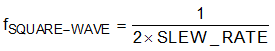
Equation 4. 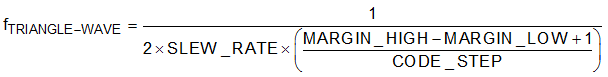
Equation 5. 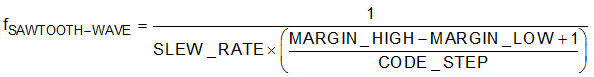
where:
- SLEW_RATE is the programmable DAC slew rate specified in Table 8-4.
- MARGIN_HIGH and MARGIN_LOW are the programmable DAC codes.
- CODE_STEP is the programmable DAC step code in Table 8-3.
Table 8-6 FUNC_CONFIG bits
| REGISTER ADDRESS AND NAME | FUNC_CONFIG[1] | FUNC_CONFIG[0] | DESCRIPTION |
|---|---|---|---|
| D1h, GENERAL_CONFIG | 0 | 0 | Generates a triangle wave between MARGIN_HIGH (address 25h) code to MARGIN_LOW (address 26h) code with slope defined by SLEW_RATE and CODE_STEP (address D1h) bits |
| 0 | 1 | Generates Saw-Tooth wave between MARGIN_HIGH (address 25h) code to MARGIN_LOW (address 26h) code, with rising slope defined by SLEW_RATE and CODE_STEP (address D1h) bits and immediate falling edge | |
| 1 | 0 | Generates Saw-Tooth wave between MARGIN_HIGH (address 25h) code to MARGIN_LOW (address 26h) code, with falling slope defined by SLEW_RATE and CODE_STEP (address D1h) bits and immediate rising edge | |
| 1 | 1 | Generates a square wave between MARGIN_HIGH (address 25h) code to MARGIN_LOW (address 26h) code with pulse high and low period defined by SLEW_RATE (address D1h) bits |