JAJSI90A November 2019 – April 2020 DAC60502 , DAC70502 , DAC80502
PRODUCTION DATA.
- 1 特長
- 2 アプリケーション
- 3 概要
- 4 改訂履歴
- 5 概要(続き)
- 6 Device Comparison Table
- 7 Pin Configuration and Functions
-
8 Specifications
- 8.1 Absolute Maximum Ratings
- 8.2 ESD Ratings
- 8.3 Recommended Operating Conditions
- 8.4 Thermal Information
- 8.5 Electrical Characteristics
- 8.6 Timing Requirements : SPI Mode
- 8.7 Timing Requirements : I2C Standard Mode
- 8.8 Timing Requirements : I2C Fast Mode
- 8.9 Timing Requirements : I2C Fast-Mode Plus
- 8.10 Typical Characteristics
-
9 Detailed Description
- 9.1 Overview
- 9.2 Functional Block Diagram
- 9.3 Feature Description
- 9.4 Device Functional Modes
- 9.5 Programming
- 9.6
Register Maps
- 9.6.1
Registers
- 9.6.1.1 NOOP Register (offset = 0h) [reset = 0000h]
- 9.6.1.2 DEVID Register (offset = 1h) [reset = 0214h for DAC80502, 1214h for DAC70502, 2214h for DAC60502]
- 9.6.1.3 SYNC Register (offset = 2h) [reset = 0300h]
- 9.6.1.4 CONFIG Register (offset = 3h) [reset = 0000h]
- 9.6.1.5 GAIN Register (offset = 4h) [reset = 0003h]
- 9.6.1.6 TRIGGER Register (offset = 5h) [reset = 0000h]
- 9.6.1.7 BRDCAST Register (offset = 6h) [reset = 0000h for RSTSEL = 0, or reset = 8000h for RSTSEL = 1]
- 9.6.1.8 STATUS Register (offset = 7h) [reset = 0000h]
- 9.6.1.9 DAC-n Register (offset = 8h–9h) [reset = 0000h for RSTSEL = 0, or reset = 8000h for RSTSEL = 1]
- 9.6.1
Registers
- 10Application and Implementation
- 11Power Supply Recommendations
- 12Layout
- 13デバイスおよびドキュメントのサポート
- 14メカニカル、パッケージ、および注文情報
9.5.1.2.2 DACx0502 I2C Update Sequence
For a single update, the DACx0502 requires a start condition, a valid I2C address byte, a command byte, and two data bytes (the most significant data byte, MSDB, and least significant data byte, LSDB), as listed in Table 2.
Table 2. Update Sequence
| MSB | .... | LSB | ACK | MSB | ... | LSB | ACK | MSB | ... | LSB | ACK | MSB | ... | LSB | ACK |
|---|---|---|---|---|---|---|---|---|---|---|---|---|---|---|---|
| Address (A) byte | Command byte | MSDB | LSDB | ||||||||||||
| DB [31:24] | DB [23:16] | DB [15:8] | DB [7:0] | ||||||||||||
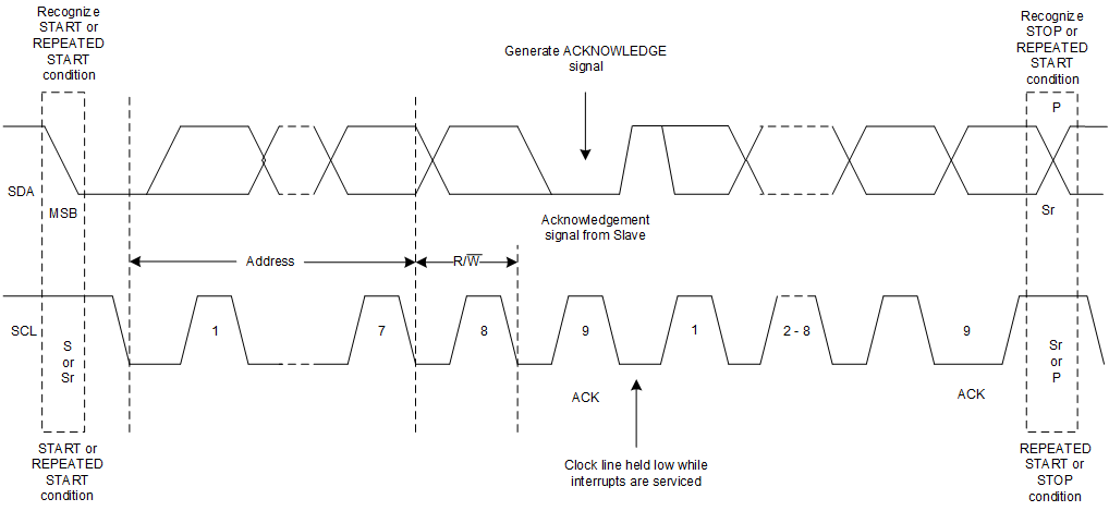
After each byte is received, the DACx0502 acknowledges the byte by pulling the SDA line low during the high period of a single clock pulse, as shown in Figure 62. These four bytes and acknowledge cycles make up the 36 clock cycles required for a single update to occur. A valid I2C™ address byte selects the DACx0502 devices.
 Figure 62. I2C Bus Protocol
 The command byte sets the operating mode of the selected DACx0502 device. When the operating mode is selected by this byte, the DACx0502 series must receive two data bytes, the most significant data byte (MSDB) and least significant data byte (LSDB), for a data update to occur. The DACx0502 devices perform an update on the falling edge of the acknowledge signal that follows the LSDB.
When using fast mode (clock = 400 kHz), the maximum DAC update rate is limited to 22.22 kSPS. Using the fast-mode plus (clock = 1 MHz), the maximum DAC update rate is limited to 55.55 kSPS. When a stop condition is received, the DACx0502 family releases the I2C bus and awaits a new start condition.