SLAS476H March 2006 – June 2017 DAC8550
PRODUCTION DATA.
- 1 Features
- 2 Applications
- 3 Description
- 4 Revision History
- 5 Pin Configuration and Functions
- 6 Specifications
- 7 Detailed Description
- 8 Application and Implementation
- 9 Power Supply Recommendations
- 10Layout
- 11Device and Documentation Support
- 12Mechanical, Packaging, and Orderable Information
1 Features
- Relative Accuracy: 8 LSB
- Glitch Energy: 0.1 nV-s
- MicroPower Operation: 140 μA at 2.7 V
- Power-On Reset to Midscale
- Power Supply: 2.7 V to 5.5 V
- 16-Bit Monotonic
- Settling Time: 10 μs to ±0.003% FSR
- Low-Power Serial Interface with Schmitt-Triggered Inputs
- On-Chip Output Buffer Amplifier with Rail-to-Rail Output Amplifier
- Power-Down Capability
- 2's Complement Input
- SYNC Interrupt Facility
- Drop-In Compatible with DAC8531/01 and DAC8551 (Binary Input)
- Available in a Tiny MSOP-8 Package
2 Applications
- Process Control
- Data Acquisition Systems
- Closed-Loop Servo-Control
- PC Peripherals
- Portable Instrumentation
- Programmable Attenuation
3 Description
The DAC8550 is a small, low-power, voltage output, 16-bit digital-to-analog converter (DAC). It is monotonic, provides good linearity, and minimizes undesired code-to-code transient voltages. The DAC8550 uses a versatile, 3-wire serial interface that operates at clock rates of up to 30 MHz and is compatible with standard SPI™, QSPI™, Microwire™, and digital signal processor (DSP) interfaces.
The DAC8550 requires an external reference voltage to set its output range. The DAC8550 incorporates a power-on reset circuit that ensures that the DAC output powers up at midscale and remains there until a valid write takes place to the device. The DAC8550 contains a power-down feature, accessed over the serial interface, that reduces the current consumption of the device to 200 nA at 5 V.
The low-power consumption of this device in normal operation makes it ideal for portable, battery-operated equipment. Power consumption is 0.38 mW at 2.7 V, reducing to less than 1 μW in power-down mode.
The DAC8550 is available in an MSOP-8 package.
For additional flexibilty, see the DAC8551, a binary-coded counterpart to the DAC8550.
Device Information(1)
| PART NUMBER | PACKAGE | BODY SIZE (NOM) |
|---|---|---|
| DAC8550 | VSSOP (8) | 3.00 mm × 3.00 mm |
- For all available packages, see the orderable addendum at the end of the data sheet.
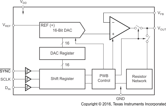
Functional Block Diagram
