SLAS476H March 2006 – June 2017 DAC8550
PRODUCTION DATA.
- 1 Features
- 2 Applications
- 3 Description
- 4 Revision History
- 5 Pin Configuration and Functions
- 6 Specifications
- 7 Detailed Description
- 8 Application and Implementation
- 9 Power Supply Recommendations
- 10Layout
- 11Device and Documentation Support
- 12Mechanical, Packaging, and Orderable Information
8 Application and Implementation
NOTE
Information in the following applications sections is not part of the TI component specification, and TI does not warrant its accuracy or completeness. TI’s customers are responsible for determining suitability of components for their purposes. Customers should validate and test their design implementation to confirm system functionality.
8.1 Application Information
The low-power consumption of the DAC8550 lends itself to applications such as loop-powered control where the current dissipation of each device is critical. The low power consumption also allows the DAC8550 to be powered using only a precision reference for increased accuracy. The low-power operation coupled with the ultra-low power power-down modes also make the DAC8550 a great choice for battery and portable applications.
8.1.1 Bipolar Operation Using DAC8550
The DAC8550 has been designed for single-supply operation, but a bipolar output range is also possible using the circuit in Figure 51. The circuit shown gives an output voltage range of ±VREF. Rail-to-rail operation at the amplifier output is achievable using an OPA703 as the output amplifier. See CMOS, Rail-to-Rail, I/O Operational Amplifier (SBOS180) for more information.
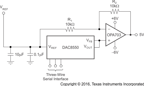 Figure 51. Bipolar Output Range
The output voltage for any input code is calculated with Equation 2 and Equation 3.

where
- D represents the input code in 2's complement (–32768 to 32767)
- VREF = 5 V
- R1 = R2 = 10 kΩ

Using this example, an output voltage range of ±5 V with 8000h corresponding to a –5-V output and 8FFFh corresponding to a 5-V output can be achieved. Similarly, using VREF = 2.5 V, a ±2.5-V output voltage range can be achieved.
8.2 Typical Applications
8.2.1 Loop-Powered 2-Wire 4-mA to 20-mA Transmitter With XTR116
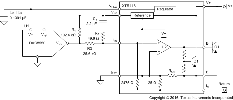 Figure 52. Loop-Powered Transmitter
8.2.1.1 Design Requirements
This design is commonly referred to as a loop-powered, or 2-wire, 4-mA to 20-mA transmitter. The transmitter has only two external input terminals: a supply connection and an output, or return, connection. The transmitter communicates back to its host, typically a PLC analog input module, by precisely controlling the magnitude of its return current. In order to conform to the 4-mA to 20-mA communication standard, the complete transmitter must consume less than 4 mA of current. The DAC8550 enables the accurate control of the loop-current from 4 mA to 20 mA in 16-bit steps.
8.2.1.2 Detailed Design Procedure
Although it is possible to recreate the loop-powered circuit using discrete components, the XTR116 provides simplicity and improved performance due to the matched internal resistors. The output current can be modified if necessary by looking using Equation 4.

For more details of this application, see 2-wire, 4-mA to 20-mA Transmitter, EMC/EMI Tested Reference Design (TIDUAO7). It covers in detail the design of this circuit as well as how to protect it from EMC/EMI tests.
8.2.2 Using REF02 as a Power Supply for DAC8550
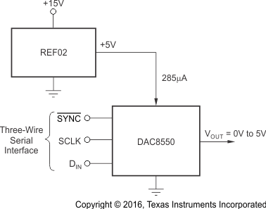 Figure 55. REF02 as a Power Supply to the DAC8550
8.2.2.1 Design Requirements
Due to the extremely low supply current required by the DAC8550, an alternative option is to use a REF02 to supply the required voltage to the device, as shown in Figure 55. See +5V Precision Voltage Reference (SBVS003) for more information.
8.2.2.2 Detailed Design Procedure
This configuration is especially useful if the power supply is quite noisy or if the system supply voltages are at some value other than 5 V. The REF02 outputs a steady supply voltage for the DAC8550. If the REF02 is used, the current it needs to supply to the DAC8550 is 250 μA. This configuration is with no load on the output of the DAC. When a DAC output is loaded, the REF02 also needs to supply the current to the load. The total typical current required (with a 5-kΩ load on the DAC output) is calculated with Equation 5.

The load regulation of the REF02 is typically 0.005%/mA, resulting in an error of 299 μV for the 1.2-mA current drawn from it. This value corresponds to an 8.9-LSB error.
8.3 System Examples
8.3.1 Microprocessor Interfacing
8.3.1.1 DAC8550 to 8051 Interface
See Figure 56 for a serial interface between the DAC8550 and a typical 8051-type microcontroller. The setup for the interface is as follows: TXD of the 8051 drives SCLK of the DAC8550, while RXD drives the serial data line of the device. The SYNC signal is derived from a bit-programmable pin on the port of the 8051. In this case, port line P3.3 is used. When data are to be transmitted to the DAC8550, P3.3 is taken LOW. The 8051 transmits data in 8-bit bytes; thus, only eight falling clock edges occur in the transmit cycle. To load data to the DAC, P3.3 is left LOW after the first eight bits are transmitted, then a second write cycle is initiated to transmit the second byte of data. P3.3 is taken HIGH following the completion of the third write cycle. The 8051 outputs the serial data in a format that has the LSB first. The DAC8550 requires its data with the MSB as the first bit received. The 8051 transmit routine must therefore take this into account, and mirror the data as needed.
 Figure 56. DAC8550 to 80C51 or 80L51 Interface
8.3.1.2 DAC8550 to Microwire Interface
Figure 57 shows an interface between the DAC8550 and any Microwire-compatible device. Serial data are shifted out on the falling edge of the serial clock and clocked into the DAC8550 on the rising edge of the SK signal.
 Figure 57. DAC8550 to Microwire Interface
8.3.1.3 DAC8550 to 68HC11 Interface
Figure 58 shows a serial interface between the DAC8550 and the 68HC11 microcontroller. SCK of the 68HC11 drives the SCLK of the DAC8550, while the MOSI output drives the serial data line of the DAC. The SYNC signal is derived from a port line (PC7), similar to the 8051 diagram.
 Figure 58. DAC8550 to 68HC11 Interface
The 68HC11 should be configured so that its CPOL bit is '0' and its CPHA bit is '1'. This configuration causes data appearing on the MOSI output to be valid on the falling edge of SCK. When data are being transmitted to the DAC, the SYNC line is held LOW (PC7). Serial data from the 68HC11 are transmitted in 8-bit bytes with only eight falling clock edges occurring in the transmit cycle. (Data are transmitted MSB first.) In order to load data to the DAC8550, PC7 is left LOW after the first eight bits are transferred, then a second and third serial write operation are performed to the DAC. PC7 is taken HIGH at the end of this procedure.
