JAJS193E April   2005  – June 2017 DAC8551

PRODUCTION DATA.  

  1. 特長
  2. アプリケーション
  3. 概要
  4. 改訂履歴
  5. Pin Configuration and Functions
  6. Specifications
    1. 6.1 Absolute Maximum Ratings
    2. 6.2 ESD Ratings
    3. 6.3 Recommended Operating Conditions
    4. 6.4 Thermal Information
    5. 6.5 Electrical Characteristics
    6. 6.6 Timing Characteristics
    7. 6.7 Typical Characteristics
      1. 6.7.1 VDD = 5 V
      2. 6.7.2 VDD = 2.7 V
  7. Detailed Description
    1. 7.1 Overview
    2. 7.2 Functional Block Diagram
    3. 7.3 Feature Description
      1. 7.3.1 DAC Section
        1. 7.3.1.1 Resistor String
        2. 7.3.1.2 Output Amplifier
      2. 7.3.2 Power-On Reset
    4. 7.4 Device Functional Modes
      1. 7.4.1 Power-Down Modes
    5. 7.5 Programming
      1. 7.5.1 Serial Interface
      2. 7.5.2 Input Shift Register
      3. 7.5.3 SYNC Interrupt
  8. Application and Implementation
    1. 8.1 Application Information
      1. 8.1.1 Bipolar Operation Using the DAC8551
    2. 8.2 Typical Application
      1. 8.2.1 Loop-Powered, 2-Wire, 4-mA to 20-mA Transmitter With XTR116
        1. 8.2.1.1 Design Requirements
        2. 8.2.1.2 Detailed Design Procedure
        3. 8.2.1.3 Application Curves
      2. 8.2.2 Using the REF02 as a Power Supply for the DAC8551
        1. 8.2.2.1 Design Requirements
        2. 8.2.2.2 Detailed Design Procedure
    3. 8.3 System Examples
      1. 8.3.1 Microprocessor Interfacing
        1. 8.3.1.1 DAC8551 to 8051 Interface
        2. 8.3.1.2 DAC8551 to Microwire Interface
        3. 8.3.1.3 DAC8551 to 68HC11 Interface
  9. Power Supply Recommendations
  10. 10Layout
    1. 10.1 Layout Guidelines
    2. 10.2 Layout Example
  11. 11デバイスおよびドキュメントのサポート
    1. 11.1 ドキュメントのサポート
      1. 11.1.1 関連資料
    2. 11.2 ドキュメントの更新通知を受け取る方法
    3. 11.3 コミュニティ・リソース
    4. 11.4 商標
    5. 11.5 静電気放電に関する注意事項
    6. 11.6 Glossary
  12. 12メカニカル、パッケージ、および注文情報

パッケージ・オプション

メカニカル・データ(パッケージ|ピン)
サーマルパッド・メカニカル・データ
発注情報

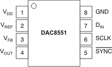
Pin Configuration and Functions

DGK Package
8-Pin VSSOP
Top View
DAC8551 po_msop_las429.gif

Pin Functions

PIN TYPE DESCRIPTION
NAME NO.
DIN 7 I Serial data input. Data is clocked into the 24-bit input shift register on each falling edge of the serial clock input. Schmitt-Trigger logic input.
GND 8 GND Ground reference point for all circuitry on the part
SCLK 6 I Serial clock input. Data can be transferred at rates up to 30-MHz Schmitt-Trigger logic input.
SYNC 5 I Level-triggered control input (active LOW). This is the frame synchronization signal for the input data. When SYNC goes LOW, it enables the input shift register and data is transferred in on the falling edges of the following clocks. The DAC is updated following the 24th clock (unless SYNC is taken HIGH before this edge, in which case the rising edge of SYNC acts as an interrupt and the write sequence is ignored by the DAC8551). Schmitt-Trigger logic input.
VDD 1 PWR Power supply input, 2.7 V to 5.5 V
VFB 3 I Feedback connection for the output amplifier. For voltage output operation, tie to VOUT externally.
VOUT 4 O Analog output voltage from DAC. The output amplifier has rail-to-rail operation.
VREF 2 I Reference voltage input