JAJS137I NOVEMBER 2006 – November 2016 DCH010505D , DCH010505S , DCH010512D , DCH010512S , DCH010515D , DCH010515S
PRODUCTION DATA.
- 1 特長
- 2 アプリケーション
- 3 概要
- 4 改訂履歴
- 5 Device Comparison Tables
- 6 Pin Configuration and Functions
- 7 Specifications
- 8 Detailed Description
- 9 Application and Implementation
- 10Power Supply Recommendations
- 11Layout
- 12デバイスおよびドキュメントのサポート
- 13メカニカル、パッケージ、および注文情報
11 Layout
11.1 Layout Guidelines
Carefully consider the layout of the PCB in order for the best results to be obtained.
Input and output power and ground planes provide a low-impedance path for the input and output power. For the output, the positive and negative voltage outputs conduct through wide traces to minimize losses.
A good-quality, low-ESR, ceramic capacitor placed as close as practical across the input reduces reflected ripple and ensure a smooth start-up.
The location of the decoupling capacitors in close proximity to their respective pins ensures low losses due to the effects of stray inductance, thus improving the ripple performance. This location is of particular importance to the input decoupling capacitor, because this capacitor supplies the transient current associated with the fast switching waveforms of the power drive circuits.
11.2 Layout Example
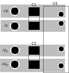
 Figure 30. DCH01 Single Output Layout
(Component-Side View)
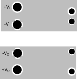
 Figure 31. DCH01 Single Output Layout
(Non-Component-Side View)