JAJSFP0F March 2016 – May 2019 DLP5530-Q1
PRODUCTION DATA.
- 1 特長
- 2 アプリケーション
- 3 概要
- 4 改訂履歴
- 5 Pin Configuration and Functions
-
6 Specifications
- 6.1 Absolute Maximum Ratings
- 6.2 Storage Conditions
- 6.3 ESD Ratings
- 6.4 Recommended Operating Conditions
- 6.5 Thermal Information
- 6.6 Electrical Characteristics
- 6.7 Timing Requirements
- 6.8 Switching Characteristics
- 6.9 System Mounting Interface Loads
- 6.10 Physical Characteristics of the Micromirror Array
- 6.11 Micromirror Array Optical Characteristics
- 6.12 Window Characteristics
- 6.13 Chipset Component Usage Specification
- 7 Detailed Description
- 8 Application and Implementation
- 9 Power Supply Recommendations
- 10Layout
- 11デバイスおよびドキュメントのサポート
- 12メカニカル、パッケージ、および注文情報
パッケージ・オプション
デバイスごとのパッケージ図は、PDF版データシートをご参照ください。
メカニカル・データ(パッケージ|ピン)
- FYK|149
サーマルパッド・メカニカル・データ
発注情報
7.1 Overview
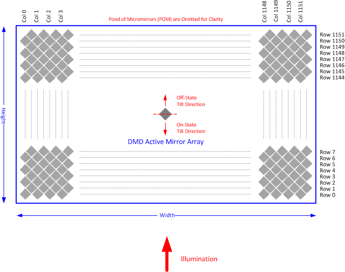
The DLP5530-Q1 Automotive DMD consists of 1,327,104 highly reflective, digitally switchable, micrometer-sized mirrors organized in a two-dimensional array. As shown in Figure 15, the micromirror array consists of 1152 micromirror columns × 1152 micromirror rows in a diamond pixel configuration with a 2:1 aspect ratio.
Around the perimeter of the 1152 × 1152 array of micromirrors is a uniform band of border micromirrors called the Pond of Micromirrors (POM). The border micromirrors are not user-addressable. The border micromirrors land in the –12° position once power has been applied to the device. There are 10 border micromirrors on each side of the 1152 × 1152 active array.
Due to the diamond pixel configuration, the columns of each odd row are offset by half a pixel from the columns of the even row. Each mirror is switchable between two discrete angular positions: –12° and +12°. The mirrors are illuminated from the bottom which allows for compact and efficient system optical design.
Although the native resolution of the DLP5530-Q1 is 1152 × 1152, when paired with the DLPC230-Q1 controller, the DLP5530-Q1 can be driven with different resolutions to utilize the 2:1 aspect ratio. For example, Head-Up Display applications typically use a resolution of 1152 × 576. Please see the DLPC230-Q1 automotive DMD controller data sheet (DLPS054) for a list of supported resolutions. Diamond pixel arrays also have the capability to increase display resolution beyond native resolution. Future controllers or video formatters may take advantage of this enhanced resolution.
 Figure 15. 0.55-in 1.3-MP Micromirror Array