DLPS053B October 2014 – October 2016
PRODUCTION DATA.
- 1 Features
- 2 Applications
- 3 Description
- 4 Revision History
- 5 Pin Configuration and Functions
-
6 Specifications
- 6.1 Absolute Maximum Ratings
- 6.2 Storage Conditions
- 6.3 ESD Ratings
- 6.4 Recommended Operating Conditions
- 6.5 Thermal Information
- 6.6 Electrical Characteristics
- 6.7 Timing Requirements
- 6.8 Typical Characteristics
- 6.9 System Mounting Interface Loads
- 6.10 Micromirror Array Physical Characteristics
- 6.11 Micromirror Array Optical Characteristics
- 6.12 Window Characteristics
- 6.13 Chipset Component Usage Specification
- 7 Detailed Description
- 8 Application and Implementation
- 9 Power Supply Requirements
- 10Layout
- 11Device Documentation Support
- 12Mechanical, Packaging, and Orderable Information
パッケージ・オプション
デバイスごとのパッケージ図は、PDF版データシートをご参照ください。
メカニカル・データ(パッケージ|ピン)
- FYE|350
サーマルパッド・メカニカル・データ
発注情報
8 Application and Implementation
NOTE
Information in the following applications sections is not part of the TI component specification, and TI does not warrant its accuracy or completeness. TI’s customers are responsible for determining suitability of components for their purposes. Customers should validate and test their design implementation to confirm system functionality.
8.1 Application Information
The DLP6500 along with the DLPC900 controller provides a solution for many applications including structured light and video projection. The DMD is a spatial light modulator, which reflects incoming light from an illumination source to one of two directions, with the primary direction being into a projection or collection optic. Each application is derived primarily from the optical architecture of the system and the format of the data coming into the DLPC900. Applications of interest include machine vision and 3D printing.
8.2 Typical Application
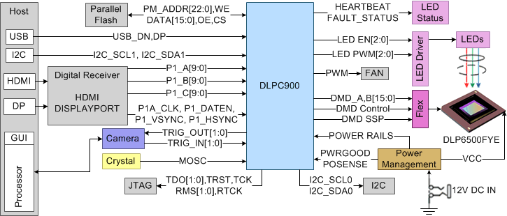
A typical embedded system application using the DLPC900 controller and a DLP6500 is shown in Figure 16. In this configuration, the DLPC900 controller supports a 24-bit parallel RGB input, typical of LCD interfaces, from an external source or processor. This system configuration supports still and motion video sources plus sequential pattern mode. Refer to Related Documents for the DLPC900 digital controller data sheet.
 Figure 16. Typical DLPC900 Application Schematic
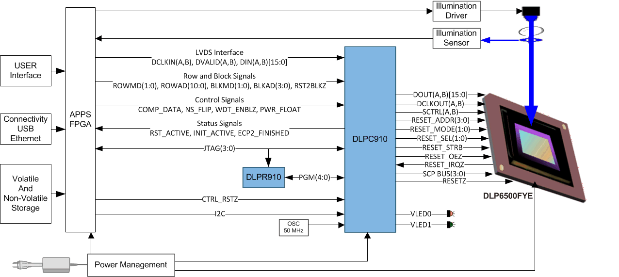
A typical embedded system application using the DLPC910 digital controller and a DLP6500 is shown in Figure 17. In this configuration, the DLPC910 digital controller accepts streaming binary patterns from an external source or processor. This system configuration supports high speed pattern mode. Refer to Related Documents for the DLPC910 digital controller datasheet.
 Figure 17. Typical DLPC910 Application Schematic
8.2.1 Design Requirements
Detailed design requirements are located in the DLPC900 digital controller data sheet. Refer to Related Documents.
8.2.2 Detailed Design Procedure
See the reference design schematic for connecting together the DLPC900 display controller and the DLP6500 DMD. An example board layout is included in the reference design data base. Layout guidelines should be followed for reliability.
See the reference design schematic for connecting together the DLPC910 controller and the DLP6500 DMD. An example board layout is included in the reference design data base. Layout guidelines should be followed for reliability.