JAJSFU7E December 2013 – March 2019 DLPC2607
PRODUCTION DATA.
- 1 特長
- 2 アプリケーション
- 3 概要
- 4 改訂履歴
- 5 Pin Configuration and Functions
-
6 Specifications
- 6.1 Absolute Maximum Ratings
- 6.2 ESD Ratings
- 6.3 Recommended Operating Conditions
- 6.4 Thermal Information
- 6.5 Typical Current and Power Dissipation
- 6.6 I/O Characteristics
- 6.7 Internal Pullup and Pulldown Characteristics
- 6.8 Parallel I/F Frame Timing Requirements
- 6.9 Parallel I/F General Timing Requirements
- 6.10 Parallel I/F Maximum Parallel Interface Horizontal Line Rate
- 6.11 BT.656 I/F General Timing Requirements
- 6.12 100- to 120-Hz Operational Limitations
- 6.13 Flash Interface Timing Requirements
- 6.14 DMD Interface Timing Requirements
- 6.15 mDDR Memory Interface Timing Requirements
- 7 Detailed Description
- 8 Application and Implementation
- 9 Power Supply Recommendations
-
10Layout
- 10.1
Layout Guidelines
- 10.1.1 Internal ASIC PLL Power
- 10.1.2 General Handling Guidelines for Unused CMOS-Type Pins
- 10.1.3 SPI Signal Routing
- 10.1.4 mDDR Memory and DMD Interface Considerations
- 10.1.5 PCB Design
- 10.1.6 General PCB Routing (Applies to All Corresponding PCB Signals)
- 10.1.7 Maximum, Pin-to-Pin, PCB Interconnects Etch Lengths
- 10.1.8 I/F Specific PCB Routing
- 10.1.9 Number of Layer Changes
- 10.1.10 Stubs
- 10.1.11 Termination Requirements:
- 10.2 Layout Example
- 10.1
Layout Guidelines
- 11デバイスおよびドキュメントのサポート
- 12メカニカル、パッケージ、および注文情報
デバイスごとのパッケージ図は、PDF版データシートをご参照ください。
メカニカル・データ(パッケージ|ピン)
- ZVB|176
サーマルパッド・メカニカル・データ
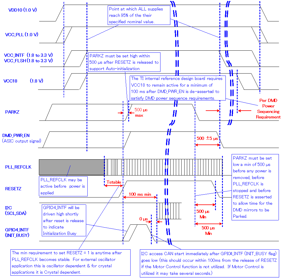
9.2 System Power-Up and Power-Down Sequence
Although the DLPC2607 device requires an array of power supply voltages, (that is, VDD, VDD_PLL, VCC_18, VCC_FLSH, and VCC_INTF), there are no restrictions regarding the relative order of power supply sequencing to avoid damaging the DLPC2607 device. This is true for both power-up and power-down scenarios. Similarly there is no minimum time between powering-up or powering-down the different supplies feeding the DLPC2607 device.
NOTE
Often, there are power sequencing requirements for devices that share the supplies with the DLPC2607 device.
From a functional standpoint, there is one specific power-sequencing recommendation to ensure proper operation. In particular, apply all ASIC power and allow it to reach the minimum specified voltage levels before RESET is deasserted to ensure proper power-up initialization is performed. Ensure that all I/O power remains applied as long as 1-V core power is applied and RESET is de-asserted.
NOTE
When VDD10 core power is applied but I/O power is not applied, additional leakage current may be drawn.
 Figure 13. Power-Up and Power-Down Timing