JAJSFU7E December 2013 – March 2019 DLPC2607
PRODUCTION DATA.
- 1 特長
- 2 アプリケーション
- 3 概要
- 4 改訂履歴
- 5 Pin Configuration and Functions
-
6 Specifications
- 6.1 Absolute Maximum Ratings
- 6.2 ESD Ratings
- 6.3 Recommended Operating Conditions
- 6.4 Thermal Information
- 6.5 Typical Current and Power Dissipation
- 6.6 I/O Characteristics
- 6.7 Internal Pullup and Pulldown Characteristics
- 6.8 Parallel I/F Frame Timing Requirements
- 6.9 Parallel I/F General Timing Requirements
- 6.10 Parallel I/F Maximum Parallel Interface Horizontal Line Rate
- 6.11 BT.656 I/F General Timing Requirements
- 6.12 100- to 120-Hz Operational Limitations
- 6.13 Flash Interface Timing Requirements
- 6.14 DMD Interface Timing Requirements
- 6.15 mDDR Memory Interface Timing Requirements
- 7 Detailed Description
- 8 Application and Implementation
- 9 Power Supply Recommendations
-
10Layout
- 10.1
Layout Guidelines
- 10.1.1 Internal ASIC PLL Power
- 10.1.2 General Handling Guidelines for Unused CMOS-Type Pins
- 10.1.3 SPI Signal Routing
- 10.1.4 mDDR Memory and DMD Interface Considerations
- 10.1.5 PCB Design
- 10.1.6 General PCB Routing (Applies to All Corresponding PCB Signals)
- 10.1.7 Maximum, Pin-to-Pin, PCB Interconnects Etch Lengths
- 10.1.8 I/F Specific PCB Routing
- 10.1.9 Number of Layer Changes
- 10.1.10 Stubs
- 10.1.11 Termination Requirements:
- 10.2 Layout Example
- 10.1
Layout Guidelines
- 11デバイスおよびドキュメントのサポート
- 12メカニカル、パッケージ、および注文情報
デバイスごとのパッケージ図は、PDF版データシートをご参照ください。
メカニカル・データ(パッケージ|ピン)
- ZVB|176
サーマルパッド・メカニカル・データ
9.4 Power-Up Initialization Sequence
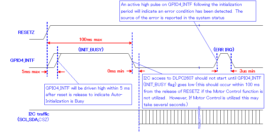
It is assumed that an external power monitor holds the DLPC2607 device in system reset during power-up. It must do this by driving RESET to a logic low state. It should continue to assert system reset until all ASIC voltages have reached minimum specified voltage levels, PARK is asserted high, and input clocks are stable. During this time, most ASIC outputs are driven to an inactive state and all bidirectional signals are configured as inputs to avoid contention. ASIC outputs that are not driven to an inactive state are tri-stated, which includes DMD_PWR_EN, LEDDVR_ON, LED_SEL_0, LED_SEL_1, SPICLK, SPIDOUT, and SPICSZ0. After power is stable and the PLL_REFCLK clock input to the DLPC2607 device is stable, then RESET should be deactivated (set to a logic high). The DLPC2607 device then performs a power-up initialization routine that first locks its PLL, followed by loading self configuration data from the external flash. Upon release of RESET, all DLPC2607 device I/Os become active. Immediately following the release of RESET, the GPIO4_INTF signal is driven high to indicate that the auto-initialization routine is in progress. Upon completion of the auto-initialization routine, the DLPC2607 device drives GPIO4_INTF low to signal INITIALIZATION DONE (also known as INIT DONE).
NOTE
The host processor can start sending standard I2C commands after GPIO4 (INIT_DONE) goes low, or a 100-ms timer expires in the host processor, whichever is earlier, irrespective of whether the motor is enabled or not. However, before sending any compound I2C commands at power-up, the host processor must wait until GPIO4 (INIT_DONE) goes low, irrespective of whether the motor control function is enabled or not. Due to motor movement, the worst-case time to wait for GPIO4 to go low is when the motor control function is enabled and system dependent; it may take several seconds.
 Figure 14. Initialization Timeline