JAJSEP0F April 2013 – May 2019 DLPC350
PRODUCTION DATA.
- 1 特長
- 2 アプリケーション
- 3 概要
- 4 改訂履歴
- 5 概要(続き)
- 6 Pin Configuration and Functions
-
7 Specifications
- 7.1 Absolute Maximum Ratings
- 7.2 ESD Ratings
- 7.3 Recommended Operating Conditions
- 7.4 Thermal Information
- 7.5 I/O Electrical Characteristics
- 7.6 I2C0 and I2C1 Interface Timing Requirements
- 7.7 Port 1 Input Pixel Interface Timing Requirements
- 7.8 Port 2 Input Pixel Interface (FPD-Link Compatible LVDS Input) Timing Requirements
- 7.9 System Oscillator Timing Requirements
- 7.10 Reset Timing Requirements
- 7.11 Video Timing Input Blanking Specification
- 7.12 Programmable Output Clocks Switching Characteristics
- 7.13 DMD Interface Switching Characteristics
- 7.14 JTAG Interface: I/O Boundary Scan Application Switching Characteristics
- 8 Parameter Measurement Information
- 9 Detailed Description
-
10Application and Implementation
- 10.1 Application Information
- 10.2 Typical Applications
- 11Power Supply Recommendations
-
12Layout
- 12.1 Layout Guidelines
- 12.2 Layout Example
- 13デバイスおよびドキュメントのサポート
- 14メカニカル、パッケージ、および注文情報
7.13 DMD Interface Switching Characteristics
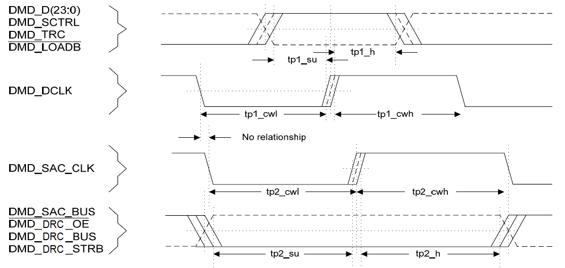
The DLPC350 controller DMD interface is comprised of a combination of both single data rate (SDR) and double data rate (DDR), and output signals using LPDDR (as defined by JESD209A). SDR signals are referenced to DMD_SAC_CLK and DDR signals are referenced to DMD_DCLK.Switching characteristics over recommended operating conditions, CL (minimum timing) = 5 pF, CL (maximum timing) = 25 pF (unless otherwise noted).
| PARAMETER | TEST CONDITIONS | FROM (INPUT) | TO (OUTPUT) | MIN | MAX | UNIT | |
|---|---|---|---|---|---|---|---|
| ƒclock1 | Clock frequency(1)(2) | N/A | DMD_DCLK | 79.992 | 120.012 | MHz | |
| tp1_clkper | Clock period | 50% reference points | N/A | DMD_DCLK | 8.332 | 12.502 | ns |
| tp1_cwh | Clock pulse duration low | 50% reference points | N/A | DMD_DCLK | 3.75 | ns | |
| tp1_cwl | Clock pulse duration high | 50% reference points | N/A | DMD_DCLK | 3.75 | ns | |
| ƒclock2 | Clock frequency(2) | N/A | DMD_SAC_CLK | 74.659 | 74.675 | MHz | |
| tp2_clkper | Clock period | 50% reference points | N/A | DMD_SAC_CLK | 13.391 | 13.394 | ns |
| tp2_cwh | Clock pulse duration low | 50% reference points | N/A | DMD_SAC_CLK | 6 | ns | |
| tp2_cwl | Clock pulse duration high | 50% reference points | N/A | DMD_SAC_CLK | 6 | ns | |
| tslew | Slew rate(3)(4)(5) | N/A | All | 0.7 | V/ns | ||
| tp1_su | Output setup time(6) | 50% reference points | Both rising and falling edges of DMD_DCLK | DMD_D(23:0), DMD_SCTRL, DMD_LOADB, DMD_TRC | 1.10 | ns | |
| tp1_h | Output hold time(6) | 50% reference points | Both rising and falling edges of DMD_DCLK | DMD_D(23:0), DMD_SCTRL, DMD_LOADB, DMD_TRC | 1.10 | ns | |
| tp1_skew | DMD data skew | 50% reference points | Relative to each other | DMD_D(23:0), DMD_SCTRL, DMD_LOADB, DMD_TRC, DMD_DCLK | 0.2 | ns | |
| tp2_su | Output setup time(6) | 50% reference points | Rising edge of DMD_SAC_CLK | DMD_SAC_BUS, DMD_DRC_OE, DMD_DRC_BUS, DMD_DRC_STRB | 2.35 | ns | |
| tp2_h | Output hold time(6) | 50% reference points | Rising edge of DMD_SAC_CLK | DMD_SAC_BUS, DMD_DRC_OE, DMD_DRC_BUS, DMD_DRC_STRB | 2.35 | ||
| tp2_skew | DRC/SAC data skew | 50% reference points | Relative to each other | DMD_SAC_BUS, DMD_DRC_OE, DMD_DRC_BUS, DMD_DRC_STRB, DMD_SAC_CLK | 0.2 | ns | |
(1) The controller supports a fixed number of programmable clock rates with the min and max values as shown. The performance may be further limited by interface voltage and PCB routing.
(2) Note that these values do not include any tolerance variation of the external crystal or oscillator, nor do they include any associated jitter.
(3) LPDDR slew rate for the rising edge is measured between VILD(DC) to VIHD(AC) where VILD(DC) = 0.3 × VDDQ and VILD(AC) = 0.8 × VDDQ.
(4) LPDDR slew rate for the rising edge is measured between VILD(DC) to VIHD(AC) where VILD(DC) = 0.7 × VDDQ and VILD(AC) = 0.2 × VDDQ.
(5) The DMD setup and hold time window must be de-rated by 300 ps for each 0.1 V/ns reduction in slew rate below 1 V/ns. Thus a 0.7 V/ns slew rate increases this window by 900 ps from 1400 to 2300 ps.
(6) The minimum output setup and hold values of the controller already include clock jitter, DCD, SSO, ISI noise, and PCB variation. In order to meet the separate setup and hold timing minimums of the DMD, only routing skew needs to be considered in system timing analysis.
 Figure 9. DMD Interface Timing