JAJSEP0F April   2013  – May 2019 DLPC350

PRODUCTION DATA.  

  1. 特長
  2. アプリケーション
  3. 概要
    1.     アプリケーション概略図
  4. 改訂履歴
  5. 概要(続き)
  6. Pin Configuration and Functions
    1.     Pin Functions
    2. Table 1. Power and Ground Pin Descriptions
  7. Specifications
    1. 7.1  Absolute Maximum Ratings
    2. 7.2  ESD Ratings
    3. 7.3  Recommended Operating Conditions
    4. 7.4  Thermal Information
    5. 7.5  I/O Electrical Characteristics
    6. 7.6  I2C0 and I2C1 Interface Timing Requirements
    7. 7.7  Port 1 Input Pixel Interface Timing Requirements
    8. 7.8  Port 2 Input Pixel Interface (FPD-Link Compatible LVDS Input) Timing Requirements
    9. 7.9  System Oscillator Timing Requirements
    10. 7.10 Reset Timing Requirements
    11. 7.11 Video Timing Input Blanking Specification
      1. 7.11.1 Source Input Blanking
    12. 7.12 Programmable Output Clocks Switching Characteristics
    13. 7.13 DMD Interface Switching Characteristics
    14. 7.14 JTAG Interface: I/O Boundary Scan Application Switching Characteristics
  8. Parameter Measurement Information
    1. 8.1 Power Consumption
  9. Detailed Description
    1. 9.1 Overview
    2. 9.2 Functional Block Diagram
    3. 9.3 Feature Description
      1. 9.3.1 Board Level Test Support
    4. 9.4 Device Functional Modes
      1. 9.4.1 Structured Light Applications
      2. 9.4.2 (LVDS) Receiver Supported Pixel Mapping Modes
  10. 10Application and Implementation
    1. 10.1 Application Information
    2. 10.2 Typical Applications
      1. 10.2.1 Typical Chipset Application
        1. 10.2.1.1 Design Requirements
        2. 10.2.1.2 Detailed Design Procedure
          1. 10.2.1.2.1 DLPC350 System Interfaces
            1. 10.2.1.2.1.1 Control Interface
            2. 10.2.1.2.1.2 Input Data Interface
          2. 10.2.1.2.2 DLPC350 System Output Interfaces
            1. 10.2.1.2.2.1 Illumination Interface
            2. 10.2.1.2.2.2 Trigger Interface (Sync Outputs)
          3. 10.2.1.2.3 DLPC350 System Support Interfaces
            1. 10.2.1.2.3.1 Reference Clock
            2. 10.2.1.2.3.2 PLL
            3. 10.2.1.2.3.3 Program Memory Flash Interface
          4. 10.2.1.2.4 DMD Interfaces
            1. 10.2.1.2.4.1 DLPC350 to DMD Digital Data
            2. 10.2.1.2.4.2 DLPC350 to DMD Control Interface
            3. 10.2.1.2.4.3 DLPC350 to DMD Micromirror Reset Control Interface
  11. 11Power Supply Recommendations
    1. 11.1 System Power and Reset
      1. 11.1.1 Default Conditions
        1. 11.1.1.1 1.2-V System Power
        2. 11.1.1.2 1.8-V System Power
        3. 11.1.1.3 1.9-V System Power
        4. 11.1.1.4 3.3-V System Power
        5. 11.1.1.5 FPD-Link Input LVDS System Power
      2. 11.1.2 System Power-up and Power-down Sequence
      3. 11.1.3 Power-On Sense (POSENSE) Support
      4. 11.1.4 Power-Good (PWRGOOD) Support
      5. 11.1.5 5-V Tolerant Support
      6. 11.1.6 Power Reset Operation
      7. 11.1.7 System Reset Operation
  12. 12Layout
    1. 12.1 Layout Guidelines
      1. 12.1.1 DMD Interface Design Considerations
      2. 12.1.2 DMD Termination Requirements
      3. 12.1.3 Decoupling Capacitors
      4. 12.1.4 Power Plane Recommendations
      5. 12.1.5 Signal Layer Recommendations
      6. 12.1.6 General Handling Guidelines for CMOS-Type Pins
      7. 12.1.7 PCB Manufacturing
        1. 12.1.7.1 General Guidelines
        2. 12.1.7.2 Trace Widths and Minimum Spacings
        3. 12.1.7.3 Routing Constraints
        4. 12.1.7.4 Fiducials
        5. 12.1.7.5 Flex Considerations
        6. 12.1.7.6 DLPC350 Thermal Considerations
    2. 12.2 Layout Example
      1. 12.2.1 Printed Circuit Board Layer Stackup Geometry
      2. 12.2.2 Recommended DLPC350 MOSC Crystal Oscillator Configuration
      3. 12.2.3 Recommended DLPC350 PLL Layout Configuration
  13. 13デバイスおよびドキュメントのサポート
    1. 13.1 デバイス・サポート
      1. 13.1.1 ビデオ・タイミング・パラメータの定義
      2. 13.1.2 デバイスの項目表記
      3. 13.1.3 デバイス・マーキング
    2. 13.2 ドキュメントのサポート
      1. 13.2.1 関連資料
    3. 13.3 商標
    4. 13.4 Glossary
  14. 14メカニカル、パッケージ、および注文情報
    1. 14.1 Package Option Addendum
      1. 14.1.1 Packaging Information

パッケージ・オプション

メカニカル・データ(パッケージ|ピン)
サーマルパッド・メカニカル・データ

FPD-Link Input LVDS System Power

The controller supports an FPD-Link compatible LVDS input for an additional method of inputting video or graphics data for display. This interface has some special controller power considerations that are separate from the other controller 1.2- or 3.3-V power rails. An FPD-Link 1.2-V power pin configuration example is shown in Figure 20.
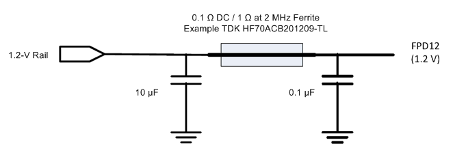
DLPC350 FPD_Link_Power_DLPS029.gifFigure 20. FPD-Link 1.2-V Power Pin Configuration

In addition, TI recommends to place the 0.1-µF low equivalent series resistance (ESR) capacitors to ground as close to the FPD-Link power pins of the DLPC350 controller as possible. FPD-Link 3.3-V power pins should also use external capacitors in the same manner as the 1.2-V pins. When FPD-Link is not utilized, the filtering can be omitted. However, the corresponding voltages must still be provided in order to avoid potential long-term reliability issues.
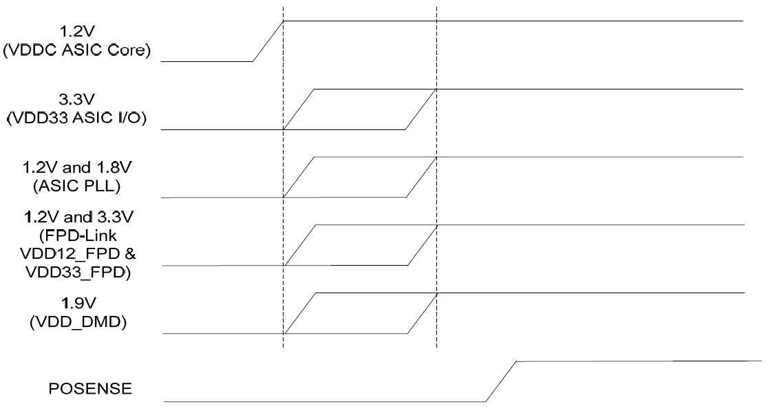
DLPC350 Power_UP_Seq_DLPS029.pngFigure 21. Initialization Timeline