JAJSEP0F April 2013 – May 2019 DLPC350
PRODUCTION DATA.
- 1 特長
- 2 アプリケーション
- 3 概要
- 4 改訂履歴
- 5 概要(続き)
- 6 Pin Configuration and Functions
-
7 Specifications
- 7.1 Absolute Maximum Ratings
- 7.2 ESD Ratings
- 7.3 Recommended Operating Conditions
- 7.4 Thermal Information
- 7.5 I/O Electrical Characteristics
- 7.6 I2C0 and I2C1 Interface Timing Requirements
- 7.7 Port 1 Input Pixel Interface Timing Requirements
- 7.8 Port 2 Input Pixel Interface (FPD-Link Compatible LVDS Input) Timing Requirements
- 7.9 System Oscillator Timing Requirements
- 7.10 Reset Timing Requirements
- 7.11 Video Timing Input Blanking Specification
- 7.12 Programmable Output Clocks Switching Characteristics
- 7.13 DMD Interface Switching Characteristics
- 7.14 JTAG Interface: I/O Boundary Scan Application Switching Characteristics
- 8 Parameter Measurement Information
- 9 Detailed Description
-
10Application and Implementation
- 10.1 Application Information
- 10.2 Typical Applications
- 11Power Supply Recommendations
-
12Layout
- 12.1 Layout Guidelines
- 12.2 Layout Example
- 13デバイスおよびドキュメントのサポート
- 14メカニカル、パッケージ、および注文情報
11.1.2 System Power-up and Power-down Sequence
Although the DLPC350 controller requires an array of power supply voltages, (for example, VDDC, VDD_1X_PLLX, VCC_18, VCC_DMD, and VCCXX_FPD), there are no restrictions regarding the relative order of power supply sequencing to avoid damaging the DLPC350 controller. This is true for both power-up and power-down. Similarly, there is no minimum time between powering-up or powering-down the different supplies of the DLPC350 controller. Note that it is not uncommon for there to be power-sequencing requirements for other devices that share power supplies with the DLPC350 controller.
Although there is no risk of damaging the DLPC350 controller as a result of a given power sequence, from a functional standpoint there are a few specific power-sequencing recommendations to ensure proper operation.
- 1.2-V core power should be applied whenever any I/O power is applied. This ensures that the powered I/O pins are set to a known state. Thus, TI recommends that core power be applied first. Other supplies should be applied only after the 1.2-V DLPC350 core has ramped up.
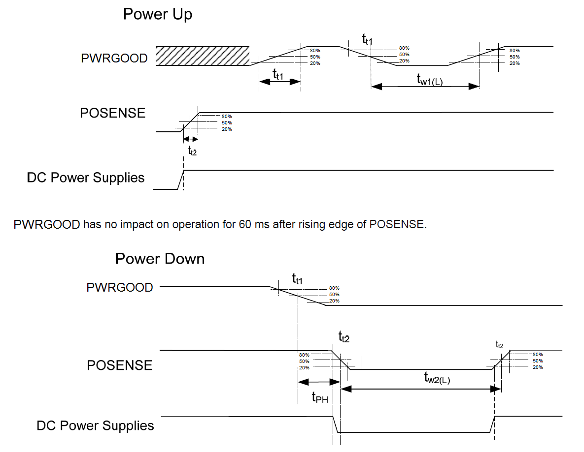
- All controller power should be applied before POSENSE is asserted to ensure proper power-up initialization is performed. 1.8-V PLL power, 1.9-V I/O power, and 3.3-V I/O power should remain applied as long as 1.2-V core power is applied and POSENSE is asserted.
It is assumed that all DLPC350 power-up sequencing is handled by external hardware. It is also assumed that an external power monitor will hold the DLPC350 controller in system reset during power-up (that is, POSENSE = 0). It should continue to assert system reset until all DLPC350 voltages have reached minimum specified voltage levels. During this time, all controller I/O are either 3-stated or driven low. The master PLL (PLLM) is released from reset upon the low-to-high transition of POSENSE, but the DLPC350 controller keeps the rest of the controller in reset for an additional 100 ms to allow the PLL to lock and stabilize its outputs. After this 100-ms delay, internal resets are de-asserted causing the microprocessor to begin its boot-up routine.
 Figure 22. Power-up and Power-down Timing