JAJSEP0F April 2013 – May 2019 DLPC350
PRODUCTION DATA.
- 1 特長
- 2 アプリケーション
- 3 概要
- 4 改訂履歴
- 5 概要(続き)
- 6 Pin Configuration and Functions
-
7 Specifications
- 7.1 Absolute Maximum Ratings
- 7.2 ESD Ratings
- 7.3 Recommended Operating Conditions
- 7.4 Thermal Information
- 7.5 I/O Electrical Characteristics
- 7.6 I2C0 and I2C1 Interface Timing Requirements
- 7.7 Port 1 Input Pixel Interface Timing Requirements
- 7.8 Port 2 Input Pixel Interface (FPD-Link Compatible LVDS Input) Timing Requirements
- 7.9 System Oscillator Timing Requirements
- 7.10 Reset Timing Requirements
- 7.11 Video Timing Input Blanking Specification
- 7.12 Programmable Output Clocks Switching Characteristics
- 7.13 DMD Interface Switching Characteristics
- 7.14 JTAG Interface: I/O Boundary Scan Application Switching Characteristics
- 8 Parameter Measurement Information
- 9 Detailed Description
-
10Application and Implementation
- 10.1 Application Information
- 10.2 Typical Applications
- 11Power Supply Recommendations
-
12Layout
- 12.1 Layout Guidelines
- 12.2 Layout Example
- 13デバイスおよびドキュメントのサポート
- 14メカニカル、パッケージ、および注文情報
11.1.7 System Reset Operation
Immediately following any type of system reset (power-up reset, PWRGOOD reset, and so forth), the DLPC350 controller automatically returns to NORMAL power mode and returns to the following state:
- All GPIO 3-state and as a result all GPIO-controlled voltage switches default to enabling power to all the DLPC350 supply lines (assuming that these outputs are externally pulled-high).
- The master PLL remains active (it is only reset on a power-up reset) and most of the derived clocks are active. However, only those resets associated with the internal processor and its peripherals are released.
- The internal processor associated clocks default to their full clock rates, as boot-up occurs at full speed.
- The PLL feeding the DDR DMD interface (PLLD) defaults to its power-down mode, and all derived clocks are inactive with the corresponding resets asserted.
- The DMD interface (except DMD_DRC_OE) default outputs to a logic low state. DMD_DRC_OE defaults to 3-state, but should be pulled high via an external 30- to 51-kΩ pullup resistor on the PCB.
- All resets output by the DLPC350 controller remain asserted until released by the internal processor (after boot-up).
- The DLPC350 controller boots-up from external flash. After the DLPC350 controller boots, it:
- Configures the programmable DDR clock generator (DCG) clock rates (that is, the DMD LPDDR interface rate).
- Enables the DCG PLL (PLLD) while holding the divider logic in reset.
- After the DCG PLL locks, the firmware sets the DMD clock rates.
- The DLPC350 firmware then releases the DCG divider logic resets, which in turn, enables all derived DCG clocks.
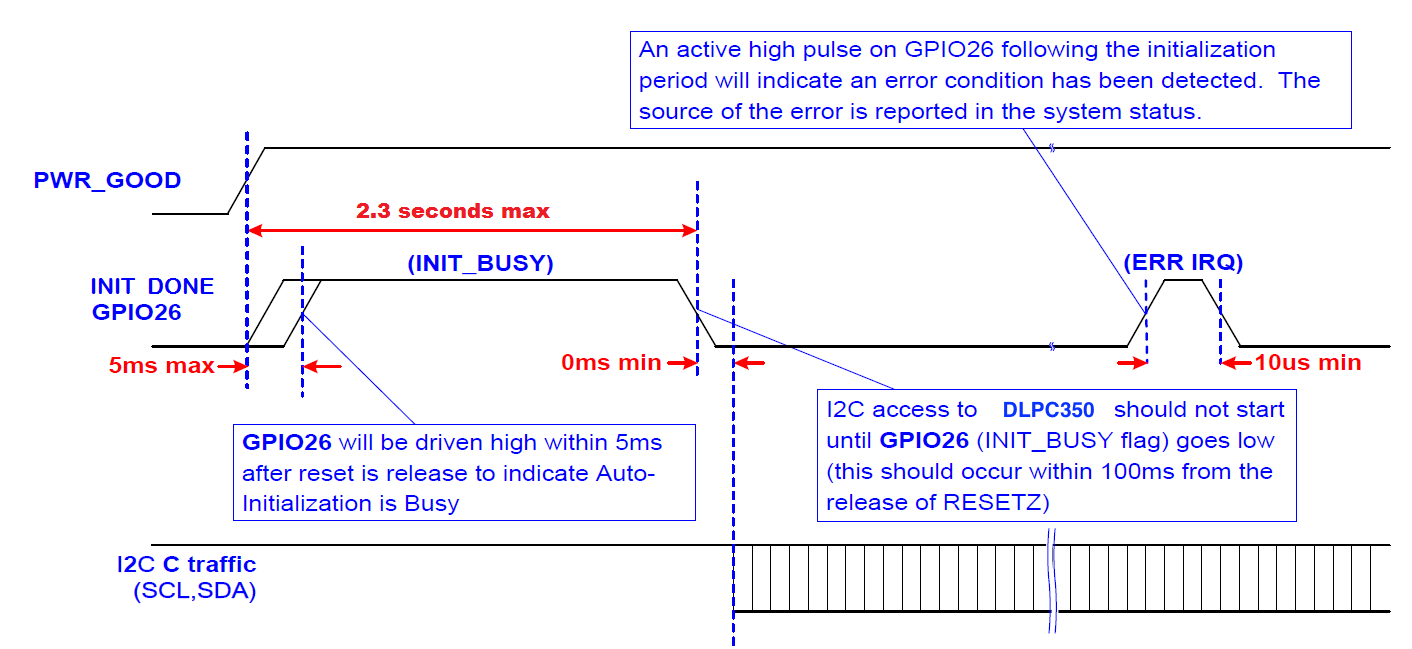
- After the clocks are configured, an internal memory test is performed. See Figure 23 and note that GPIO26 is the INIT_DONE signal.
Application software should wait for a wake-up command from the user. After the controller is requested to wake-up, the software should place the controller back in NORMAL mode and re-initialize clocks and resets as required. See reset timing requirements in Reset Timing Requirements.
 Figure 23. Internal Memory Test Diagram