JAJSDU1 August 2017 DRV5012
PRODUCTION DATA.
- 1 特長
- 2 アプリケーション
- 3 概要
- 4 改訂履歴
- 5 Pin Configuration and Functions
- 6 Specifications
- 7 Detailed Description
- 8 Application and Implementation
- 9 Power Supply Recommendations
- 10Layout
- 11デバイスおよびドキュメントのサポート
- 12メカニカル、パッケージ、および注文情報
パッケージ・オプション
デバイスごとのパッケージ図は、PDF版データシートをご参照ください。
メカニカル・データ(パッケージ|ピン)
- DMR|4
サーマルパッド・メカニカル・データ
- DMR|4
発注情報
6 Specifications
6.1 Absolute Maximum Ratings
over operating free-air temperature range (unless otherwise noted)(1)| MIN | MAX | UNIT | |||
|---|---|---|---|---|---|
| Power supply voltage | VCC | –0.3 | 5.5 | V | |
| Power supply voltage slew rate | VCC | Unlimited | V / µs | ||
| Output voltage | OUT | –0.3 | VCC + 0.3 | V | |
| Output current | OUT | –5 | 5 | mA | |
| Input voltage | SEL | –0.3 | VCC + 0.3 | V | |
| Magnetic flux density, BMAX | Unlimited | T | |||
| Junction temperature, TJ | 105 | °C | |||
| Storage temperature, Tstg | –65 | 150 | °C | ||
(1) Stresses beyond those listed under Absolute Maximum Ratings may cause permanent damage to the device. These are stress ratings only, which do not imply functional operation of the device at these or any other conditions beyond those indicated under Recommended Operating Conditions. Exposure to absolute-maximum-rated conditions for extended periods may affect device reliability.
6.2 ESD Ratings
| VALUE | UNIT | |||
|---|---|---|---|---|
| V(ESD) | Electrostatic discharge | Human-body model (HBM), per ANSI/ESDA/JEDEC JS-001(1) | ±6000 | V |
| Charged-device model (CDM), per JEDEC specification JESD22-C101(2) | ±750 | |||
(1) JEDEC document JEP155 states that 500-V HBM allows safe manufacturing with a standard ESD control process.
(2) JEDEC document JEP157 states that 250-V CDM allows safe manufacturing with a standard ESD control process.
6.3 Recommended Operating Conditions
over operating free-air temperature range (unless otherwise noted)| MIN | MAX | UNIT | ||
|---|---|---|---|---|
| VCC | Power supply voltage (VCC) | 1.65 | 5.5 | V |
| VO | Output voltage (OUT) | 0 | VCC | V |
| IO | Output current (OUT) | –5 | 5 | mA |
| VI | Input voltage (SEL) | 0 | VCC | V |
| TA | Operating ambient temperature | –40 | 85 | °C |
6.4 Thermal Information
| THERMAL METRIC(1) | DRV5012 | UNIT | |
|---|---|---|---|
| DMR (X2SON) | |||
| 4 PINS | |||
| RθJA | Junction-to-ambient thermal resistance | 159 | °C/W |
| RθJC(top) | Junction-to-case (top) thermal resistance | 77 | °C/W |
| RθJB | Junction-to-board thermal resistance | 102 | °C/W |
| ψJT | Junction-to-top characterization parameter | 0.9 | °C/W |
| ψJB | Junction-to-board characterization parameter | 100 | °C/W |
(1) For more information about traditional and new thermal metrics, see the Semiconductor and IC Package Thermal Metrics application report.
6.5 Electrical Characteristics
for VCC = 1.65 V to 5.5 V, over operating free-air temperature range (unless otherwise noted)| PARAMETER | TEST CONDITIONS | MIN | TYP | MAX | UNIT | ||
|---|---|---|---|---|---|---|---|
| OUT pin | |||||||
| VOH | High-level output voltage | IOUT = –1 mA | VCC – 0.35 | VCC – 0.1 | V | ||
| VOL | Low-level output voltage | IOUT = 1 mA | 0.1 | 0.3 | V | ||
| SEL pin | |||||||
| VIH | High-level input voltage | VCC = 1.65 to 2.5 V | 0.8 × VCC | V | |||
| VCC = 2.5 to 5.5 V | 2 | ||||||
| VIL | Low-level input voltage | 0.15 × VCC | V | ||||
| IIH | High-level input leakage current | SEL = VCC | 1 | nA | |||
| IIL | Low-level input leakage current | SEL = 0 V | 1 | nA | |||
| DYNAMIC CHARACTERISTICS | |||||||
| fS | Frequency of magnetic sampling | SEL = Low | 13.3 | 20 | 37 | Hz | |
| SEL = High | 1665 | 2500 | 4700 | ||||
| tS | Period of magnetic sampling | SEL = Low | 27 | 50 | 75 | ms | |
| SEL = High | 0.21 | 0.4 | 0.6 | ||||
| ICC(AVG) | Average current consumption | VCC = 1.8 V | SEL = Low | 1.3 | µA | ||
| SEL = High | 142 | ||||||
| VCC = 3 V | SEL = Low | 1.6 | 3.3 | ||||
| SEL = High | 153 | 370 | |||||
| VCC = 5 V | SEL = Low | 2 | |||||
| SEL = High | 160 | ||||||
| ICC(PK) | Peak current consumption | 2 | 2.7 | mA | |||
| tON | Power-on time (see Figure 11) | 55 | 100 | µs | |||
| tACTIVE | Active time period (see Figure 11) | 40 | µs | ||||
6.6 Magnetic Characteristics
for VCC = 1.65 V to 5.5 V, over operating free-air temperature range (unless otherwise noted)| PARAMETER | TEST CONDITIONS | MIN | TYP | MAX | UNIT | |
|---|---|---|---|---|---|---|
| BOP | Magnetic threshold operate point (see Figure 9) | 0.6 | 2 | 3.3 | mT | |
| BRP | Magnetic threshold release point (see Figure 9) | –3.3 | –2 | –0.6 | mT | |
| BHYS | Magnetic hysteresis: |BOP – BRP| | 2 | 4 | mT | ||
6.7 Typical Characteristics
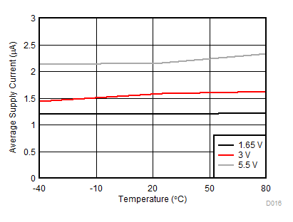 Figure 1. ICC(AVG) vs Temperature (20-Hz Mode)
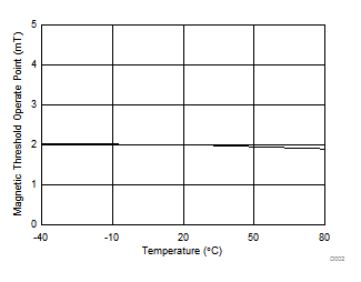 Figure 3. BOP vs Temperature
 Figure 5. BOP vs VCC
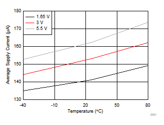 Figure 2. ICC(AVG) vs Temperature (2.5-kHz Mode)
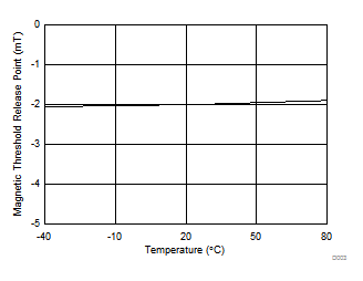 Figure 4. BRP vs Temperature
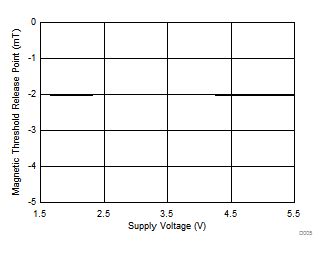 Figure 6. BRP vs VCC