JAJSDU1 August 2017 DRV5012
PRODUCTION DATA.
- 1 特長
- 2 アプリケーション
- 3 概要
- 4 改訂履歴
- 5 Pin Configuration and Functions
- 6 Specifications
- 7 Detailed Description
- 8 Application and Implementation
- 9 Power Supply Recommendations
- 10Layout
- 11デバイスおよびドキュメントのサポート
- 12メカニカル、パッケージ、および注文情報
パッケージ・オプション
デバイスごとのパッケージ図は、PDF版データシートをご参照ください。
メカニカル・データ(パッケージ|ピン)
- DMR|4
サーマルパッド・メカニカル・データ
- DMR|4
発注情報
7 Detailed Description
7.1 Overview
The DRV5012 device is a magnetic sensor with a digital output that latches the most recent pole measured. Applying a south magnetic pole near the top of the package causes the output to drive low, a north pole causes the output to drive high, and the absence of a magnetic field causes the output to continue to drive the previous state, whether low or high.
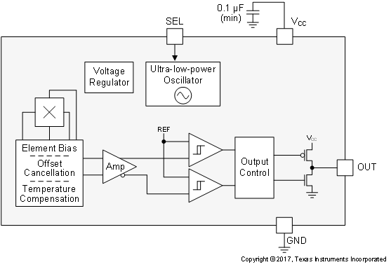
The device integrates a Hall effect element, analog signal conditioning, and a low-frequency oscillator that enables ultra-low average power consumption. By operating from a 1.65-V to 5.5-V supply, the device periodically measures magnetic flux density, updates the output, and enters a low-power sleep state. A logic input pin, SEL, sets the sampling frequency to 20 Hz or 2.5 kHz with a tradeoff in power consumption.
7.2 Functional Block Diagram
7.3 Feature Description
7.3.1 Magnetic Flux Direction
The DRV5012 device is sensitive to the magnetic field component that is perpendicular to the top of the package (as shown in Figure 7).
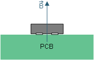 Figure 7. Direction of Sensitivity
Magnetic flux that travels from the bottom to the top of the package is considered positive in this data sheet. This condition exists when a south magnetic pole is near the top of the package. Magnetic flux that travels from the top to the bottom of the package results in negative millitesla values.
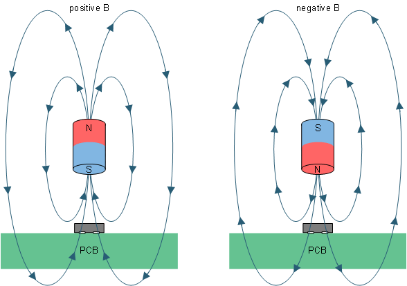 Figure 8. Flux Direction Polarity
7.3.2 Magnetic Response
Figure 9 shows the device functionality and hysteresis.
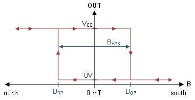 Figure 9. Device Functionality
7.3.3 Output Driver
The device features a push-pull CMOS output that can drive a VCC or ground level.
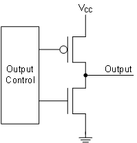 Figure 10. Push-Pull Output (Simplified)
7.3.4 Sampling Rate
When the DRV5012 device powers up, it measures the first magnetic sample and sets the output within the tON time. The output is latched, and the device enters an ultra-low-power sleep state. After each tS time has passed, the device measures a new sample and updates the output if necessary. If the magnetic field does not change between periods, the output also does not change.
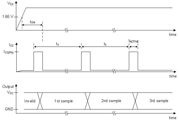 Figure 11. Timing Diagram
7.3.5 SEL Pin
The SEL pin is a CMOS input that selects between two sampling rates. When the pin is low, the device samples at 20 Hz and uses low power. When the pin is high, the device samples at 2500 Hz and uses more power. The SEL pin can be tied directly high or low, or it can be changed during device operation. If the SEL voltage changes, the device detects the new voltage during the next tACTIVE time.
7.3.6 Hall Element Location
The sensing element inside the device is in the center of the package when viewed from the top. Figure 12 shows the tolerances and side-view dimensions.
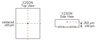 Figure 12. Hall Element Location
7.4 Device Functional Modes
The DRV5012 device has two operating modes, 20 Hz and 2.5 kHz, as set by the SEL pin. In both cases the Recommended Operating Conditions must be met.