JAJSEF0C October   2017  – July 2018 DRV5055-Q1

PRODUCTION DATA.  

  1. 特長
  2. アプリケーション
  3. 概要
    1.     Device Images
      1.      標準的な回路図
      2.      磁気応答(A1、A2、A3、A4バージョン)
  4. 改訂履歴
  5. Pin Configuration and Functions
    1.     Pin Functions
  6. Specifications
    1. 6.1 Absolute Maximum Ratings
    2. 6.2 ESD Ratings
    3. 6.3 Recommended Operating Conditions
    4. 6.4 Thermal Information
    5. 6.5 Electrical Characteristics
    6. 6.6 Magnetic Characteristics
    7. 6.7 Typical Characteristics
  7. Detailed Description
    1. 7.1 Overview
    2. 7.2 Functional Block Diagram
    3. 7.3 Feature Description
      1. 7.3.1 Magnetic Flux Direction
      2. 7.3.2 Magnetic Response
      3. 7.3.3 Sensitivity Linearity
      4. 7.3.4 Ratiometric Architecture
      5. 7.3.5 Operating VCC Ranges
      6. 7.3.6 Sensitivity Temperature Compensation for Magnets
      7. 7.3.7 Power-On Time
      8. 7.3.8 Hall Element Location
    4. 7.4 Device Functional Modes
  8. Application and Implementation
    1. 8.1 Application Information
      1. 8.1.1 Selecting the Sensitivity Option
      2. 8.1.2 Temperature Compensation for Magnets
      3. 8.1.3 Adding a Low-Pass Filter
      4. 8.1.4 Designing for Wire Break Detection
    2. 8.2 Typical Application
      1. 8.2.1 Design Requirements
      2. 8.2.2 Detailed Design Procedure
      3. 8.2.3 Application Curve
    3. 8.3 Do's and Don'ts
  9. Power Supply Recommendations
  10. 10Layout
    1. 10.1 Layout Guidelines
    2. 10.2 Layout Examples
  11. 11デバイスおよびドキュメントのサポート
    1. 11.1 ドキュメントのサポート
      1. 11.1.1 関連資料
    2. 11.2 ドキュメントの更新通知を受け取る方法
    3. 11.3 コミュニティ・リソース
    4. 11.4 商標
    5. 11.5 静電気放電に関する注意事項
    6. 11.6 Glossary
  12. 12メカニカル、パッケージ、および注文情報

パッケージ・オプション

メカニカル・データ(パッケージ|ピン)
サーマルパッド・メカニカル・データ
発注情報

Sensitivity Linearity

The device produces a linear response when the output voltage is within the specified VL range. Outside this range, sensitivity is reduced and nonlinear. Figure 16 and Figure 17 graph the magnetic response.
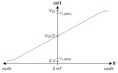
DRV5055-Q1 graph.gifFigure 16. Magnetic Response of the A1, A2, A3, A4 Versions
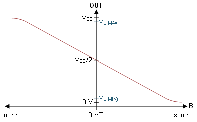
DRV5055-Q1 graphA5.gifFigure 17. Magnetic Response of the A5 Version

Equation 2 calculates parameter BL, the minimum linear sensing range at 25°C taking into account the maximum quiescent voltage and sensitivity tolerances.

Equation 2. DRV5055-Q1 BLeq.gif

The parameter SLE defines linearity error as the difference in sensitivity between any two positive B values, and any two negative B values, while the output is within the VL range.

The parameter SSE defines symmetry error as the difference in sensitivity between any positive B value and the negative B value of the same magnitude, while the output voltage is within the VL range.