SLES267C August   2011  – March 2016 DRV8302

PRODUCTION DATA.  

  1. Features
  2. Applications
  3. Description
  4. Revision History
  5. Pin Configuration and Functions
  6. Specifications
    1. 6.1 Absolute Maximum Ratings
    2. 6.2 ESD Ratings
    3. 6.3 Recommended Operating Conditions
    4. 6.4 Thermal Information
    5. 6.5 Electrical Characteristics
    6. 6.6 Gate Timing and Protection Characteristics
    7. 6.7 Current Shunt Amplifier Characteristics
    8. 6.8 Buck Converter Characteristics
    9. 6.9 Typical Characteristics
  7. Detailed Description
    1. 7.1 Overview
    2. 7.2 Function Block Diagram
    3. 7.3 Feature Description
      1. 7.3.1 Three-Phase Gate Driver
      2. 7.3.2 Current Shunt Amplifiers
      3. 7.3.3 Buck Converter
      4. 7.3.4 Protection Features
        1. 7.3.4.1 Overcurrent Protection (OCP) and Reporting
          1. 7.3.4.1.1 Current Limit Mode (M_OC = LOW)
          2. 7.3.4.1.2 OC Latch Shutdown Mode
        2. 7.3.4.2 OC_ADJ
        3. 7.3.4.3 Undervoltage Protection (UVLO)
        4. 7.3.4.4 Overvoltage Protection (GVDD_OV)
        5. 7.3.4.5 Overtemperature Protection
        6. 7.3.4.6 Fault and Protection Handling
    4. 7.4 Device Functional Modes
      1. 7.4.1 EN_GATE
      2. 7.4.2 DTC
  8. Application and Implementation
    1. 8.1 Application Information
      1. 8.1.1 Gate Driver Power Up Sequencing Errdata
    2. 8.2 Typical Application
      1. 8.2.1 Design Requirements
      2. 8.2.2 Detailed Design Procedure
        1. 8.2.2.1 Gate Drive Average Current Load
        2. 8.2.2.2 Overcurrent Protection Setup
        3. 8.2.2.3 Sense Amplifier Setup
      3. 8.2.3 Application Curves
  9. Power Supply Recommendations
    1. 9.1 Bulk Capacitance
  10. 10Layout
    1. 10.1 Layout Guidelines
    2. 10.2 Layout Example
  11. 11Device and Documentation Support
    1. 11.1 Documentation Support
      1. 11.1.1 Related Documentation
    2. 11.2 Community Resources
    3. 11.3 Trademarks
    4. 11.4 Electrostatic Discharge Caution
    5. 11.5 Glossary
  12. 12Mechanical, Packaging, and Orderable Information

パッケージ・オプション

メカニカル・データ(パッケージ|ピン)
サーマルパッド・メカニカル・データ
発注情報

10 Layout

10.1 Layout Guidelines

Use these layout recommendations when designing a PCB for the DRV8302.

  • The DRV8302 makes an electrical connection to GND through the PowerPAD. Always check to ensure that the PowerPAD has been properly soldered (See the application report, PowerPAD™ Thermally Enhanced Package application report, SLMA002).
  • PVDD bypass capacitors should be placed close to their corresponding pins with a low impedance path to device GND (PowerPAD).
  • GVDD bypass capacitor should be placed close its corresponding pin with a low impedance path to device GND (PowerPAD).
  • AVDD and DVDD bypass capacitors should be placed close to their corresponding pins with a low impedance path to the AGND pin. It is preferable to make this connection on the same layer.
  • AGND should be tied to device GND (PowerPAD) through a low impedance trace/copper fill.
  • Add stitching vias to reduce the impedance of the GND path from the top to bottom side.
  • Try to clear the space around and underneath the DRV8302 to allow for better heat spreading from the PowerPAD.

10.2 Layout Example
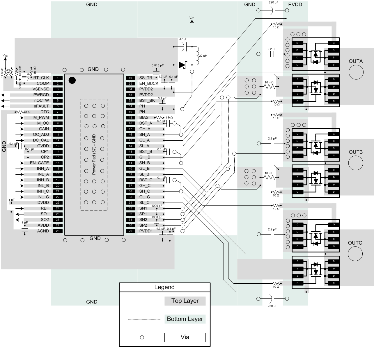
DRV8302 layout_2_sles267.gif Figure 12. Top and Bottom Layer Layout Schematic