SLVSCX5B March 2015 – July 2015 DRV8701
PRODUCTION DATA.
- 1 Features
- 2 Applications
- 3 Description
- 4 Revision History
- 5 Pin Configuration and Functions
- 6 Specifications
-
7 Detailed Description
- 7.1 Overview
- 7.2 Functional Block Diagram
- 7.3
Feature Description
- 7.3.1 Bridge Control
- 7.3.2 Half-Bridge Operation
- 7.3.3 Current Regulation
- 7.3.4 Amplifier Output SO
- 7.3.5 PWM Motor Gate Drivers
- 7.3.6 IDRIVE Pin
- 7.3.7 Dead Time
- 7.3.8 Propagation Delay
- 7.3.9 Overcurrent VDS Monitor
- 7.3.10 Charge Pump
- 7.3.11 LDO Voltage Regulators
- 7.3.12 Gate Drive Clamp
- 7.3.13 Protection Circuits
- 7.3.14 Reverse Supply Protection
- 7.4 Device Functional Modes
- 8 Application and Implementation
- 9 Power Supply Recommendations
- 10Layout
- 11Device and Documentation Support
- 12Mechanical, Packaging, and Orderable Information
1 Features
- Single H-Bridge Gate Driver
- Drives Four External N-Channel MOSFETs
- Supports 100% PWM Duty Cycle
- 5.9-V to 45-V Operating Supply Voltage Range
- Two Control Interface Options
- PH/EN (DRV8701E)
- PWM (DRV8701P)
- Adjustable Gate Drive (5 Levels)
- 6-mA to 150-mA Source Current
- 12.5-mA to 300-mA Sink Current
- Supports 1.8-V, 3.3-V, and 5-V Logic Inputs
- Current Shunt Amplifier (20 V/V)
- Integrated PWM Current Regulation
- Limits Motor Inrush Current
- Low-Power Sleep Mode (9 μA)
- Two LDO Voltage Regulators to Power External Components
- AVDD: 4.8 V, up to 30-mA Output Load
- DVDD: 3.3 V, up to 30-mA Output Load
- Small Package and Footprint
- 24-Pin VQFN (PowerPAD™)
- 4.0 × 4.0 × 0.9 mm
- Protection Features:
- VM Undervoltage Lockout (UVLO)
- Charge Pump Undervoltage (CPUV)
- Overcurrent Protection (OCP)
- Pre-Driver Fault (PDF)
- Thermal Shutdown (TSD)
- Fault Condition Output (nFAULT)
2 Applications
- Industrial Brushed-DC Motors
- Robotics
- Home Automation
- Industrial Pumps and Valves
- Power Tools
- Handheld Vacuum Cleaners
3 Description
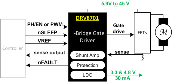
The DRV8701 is a single H-bridge gate driver that uses four external N-channel MOSFETs targeted to drive a 12-V to 24-V bidirectional brushed DC motor.
A PH/EN (DRV8701E) or PWM (DRV8701P) interface allows simple interfacing to controller circuits. An internal sense amplifier allows for adjustable current control. The gate driver includes circuitry to regulate the winding current using fixed off-time PWM current chopping.
DRV8701 drives both high- and low-side FETs with 9.5-V VGS gate drive. The gate drive current for all external FETs is configurable with a single external resistor on the IDRIVE pin.
A low-power sleep mode is provided which shuts down internal circuitry to achieve very-low quiescent current draw. This sleep mode can be set by taking the nSLEEP pin low.
Internal protection functions are provided: undervoltage lockout, charge pump faults, overcurrent shutdown, short-circuit protection, predriver faults, and overtemperature. Fault conditions are indicated on the nFAULT pin.
Device Information(1)
| PART NUMBER | PACKAGE | BODY SIZE (NOM) |
|---|---|---|
| DRV8701 | VQFN (24) | 4.00 × 4.00 x 0.90 mm |
- For all available packages, see the orderable addendum at the end of the data sheet.
SPACE
Simplified System Block Diagram

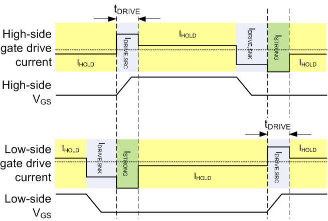
Gate-Drive Current
