JAJSI17D November 2013 – October 2019 DRV8850
PRODUCTION DATA.
- 1 特長
- 2 アプリケーション
- 3 概要
- 4 改訂履歴
- 5 Pin Configuration and Functions
- 6 Specifications
-
7 Detailed Description
- 7.1 Overview
- 7.2 Functional Block Diagram
- 7.3 Feature Description
- 7.4 Device Functional Modes
- 8 Application and Implementation
- 9 Power Supply Recommendations
- 10Layout
- 11デバイスおよびドキュメントのサポート
- 12メカニカル、パッケージ、および注文情報
パッケージ・オプション
メカニカル・データ(パッケージ|ピン)
- RGY|24
サーマルパッド・メカニカル・データ
- RGY|24
発注情報
7.3.6 Propagation Delay
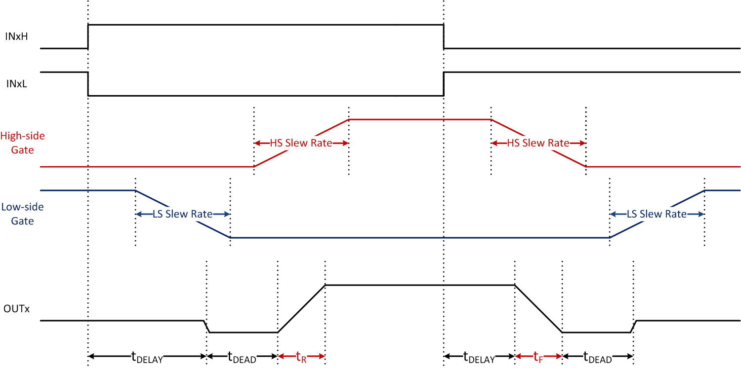
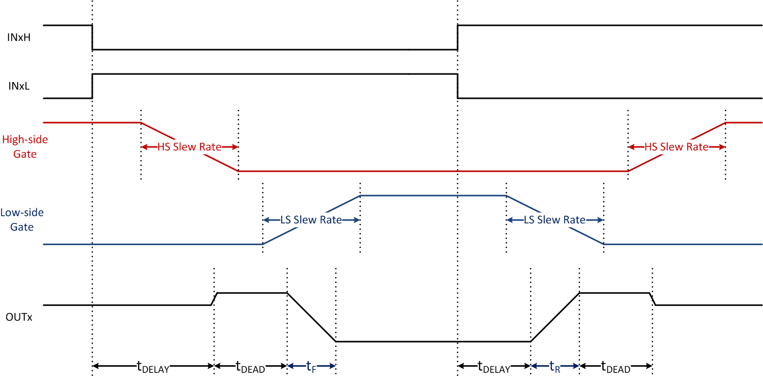
The propagation delay time (tDELAY) is measured as the time between an input edge to an output change. This time is composed of two parts: an input deglitcher and output slewing delay. The input deglitcher prevents noise on the input pins from affecting the output state.
The output slew rate also contributes to the delay time. For the output to change state during typical operation, first one FET must be turned off. The FET gate is ramped down according to the SR resistor selection, and the observed propagation delay ends when the FET gate falls to less than the threshold voltage.
 Figure 16. Low-Side Slow Decay Operation – Current Sourced from OUTx
  Figure 17. High-Side Slow Decay or Fast Decay Operation – Current Sunk into OUTx