SLRS065E September 2013 – November 2015 DRV8860
PRODUCTION DATA.
- 1 Features
- 2 Applications
- 3 Description
- 4 Simplified Schematic
- 5 Revision History
- 6 Pin Configuration and Functions
- 7 Specifications
- 8 Detailed Description
- 9 Application and Implementation
- 10Power Supply Recommendations
- 11Layout
- 12Device and Documentation Support
- 13Mechanical, Packaging, and Orderable Information
パッケージ・オプション
メカニカル・データ(パッケージ|ピン)
サーマルパッド・メカニカル・データ
- PWP|16
発注情報
7 Specifications
7.1 Absolute Maximum Ratings
over operating free-air temperature range (unless otherwise noted) (1) (2) (3)| MIN | MAX | UNIT | ||
|---|---|---|---|---|
| Power supply voltage range | VM | –0.3 | 40 | V |
| Digital input pin current range | ENABLE, LATCH, CLK, DIN | 0 | 20 | mA |
| Digital output pin voltage range | DOUT, nFAULT | –0.5 | 7 | V |
| Digital output pin current | DOUT, nFAULT | –0.5 | 7 | V |
| Output voltage range | OUTx | –0.3 | 40 | V |
| Output current range | OUTx | Internally limited | A | |
| Operating virtual junction temperature range, TJ | –40 | 150 | °C | |
(1) Stresses beyond those listed under “absolute maximum ratings” may cause permanent damage to the device. These are stress ratings only, and functional operation of the device at these or any other conditions beyond those indicated under “recommended operating conditions” is not implied. Exposure to absolute–maximum–rated conditions for extended periods may affect device reliability.
(2) All voltage values are with respect to network ground terminal.
(3) Power dissipation and thermal limits must be observed
7.2 Handling Ratings
| MIN | MAX | UNIT | |||
|---|---|---|---|---|---|
| Tstg | Storage temperature range | –60 | 150 | °C | |
| V(ESD) | Electrostatic discharge | Human body model (HBM), per ANSI/ESDA/JEDEC JS-001, all pins (1) | –2 | 2 | kV |
| Charged device model (CDM), per JEDEC specification JESD22-C101, all pins (2) | –500 | 500 | V | ||
(1) JEDEC document JEP155 states that 500-V HBM allows safe manufacturing with a standard ESD control process.
(2) JEDEC document JEP157 states that 250-V CDM allows safe manufacturing with a standard ESD control process.
7.3 Recommended Operating Conditions
over operating free-air temperature range (unless otherwise noted)| MIN | NOM | MAX | UNIT | ||
|---|---|---|---|---|---|
| VM | Motor power supply voltage range | 8 | 38 | V | |
| IOUT | Low-side driver current capability | 560 | mA | ||
| TA | Operating ambient temperature range | –40 | 85 | °C | |
7.4 Thermal Information (1)
over operating free-air temperature range (unless otherwise noted)| THERMAL METRIC | TSSOP | HTSSOP | UNIT | |
|---|---|---|---|---|
| PW (16 PINS) | PWP (16 PINS) | |||
| ΘJA | Junction-to-ambient thermal resistance | 103 | 40.9 | °C/W |
| RθJC(TOP) | Junction-to-case (top) thermal resistance | 37.9 | 28.5 | °C/W |
| RθJB | Junction-to-board thermal resistance | 48 | 23.2 | °C/W |
| ΨJT | Junction-to-top characterization parameter | 3 | 0.9 | °C/W |
| ΨJB | Junction-to-board characterization parameter | 47.4 | 23.0 | °C/W |
| RθJC(BOTTOM) | Junction-to-case (bottom) thermal resistance | N/A | 3.0 | °C/W |
(1) For more information about traditional and new thermal metrics, see the IC Package Thermal Metrics application report, SPRA953.
7.5 Electrical Characteristics
TA = 25°C, over operating free-air temperature range (unless otherwise noted)7.6 Timing Requirements
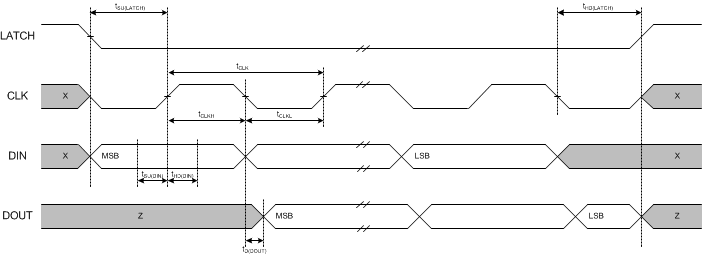
 Figure 1. Serial Interface
Table 2. Serial Timing
| NO. | REF DES | DESCRIPTION | MIN | TYP | MAX | UNIT |
|---|---|---|---|---|---|---|
| 1 | tCLK | CLK cycle time | 5 | µs | ||
| 2 | tCLKH | CLK high time | 2.5 | µs | ||
| 3 | tCLKL | CLK low time | 2.5 | µs | ||
| 4 | tSU(DIN) | Setup time, DIN to CLK | 1 | µs | ||
| 5 | tH(DIN) | Hold time, DIN to CLK | 1 | µs | ||
| 6 | tSU(LATCH) | Setup time, LATCH to CLK | 1 | µs | ||
| 7 | tH(LATCH) | Hold time, LATCH to CLK | 1 | µs | ||
| 8 | tOFF(LATCH) | Inactive time between writes and read | 2 | µs | ||
| 9 | tD(DOUT) | Delay time, CLK to DOUT | 1.5 | µs |
 Figure 2. Special Commands
Table 3. Special Commands
| NO. | REF DES | DESCRIPTION | MIN | TYP | MAX | UNIT |
|---|---|---|---|---|---|---|
| 10 | tf(LATCH) | LATCH fall to CLK rise | 1 | µs | ||
| 11 | tr(LATCH) | CLK fall to LATCH rise | 1 | µs | ||
| 12 | tH(LATCH) | LATCH high time | 2 | µs |

