SLVSD18C June 2015 – August 2017 DRV8880
PRODUCTION DATA.
- 1 Features
- 2 Applications
- 3 Description
- 4 Revision History
- 5 Pin Configuration and Functions
- 6 Specifications
-
7 Detailed Description
- 7.1 Overview
- 7.2 Functional Block Diagram
- 7.3
Feature Description
- 7.3.1 Stepper Motor Driver Current Ratings
- 7.3.2 PWM Motor Drivers
- 7.3.3 Microstepping Indexer
- 7.3.4 Current Regulation
- 7.3.5
Decay Modes
- 7.3.5.1 Mode 1: Slow Decay for Increasing and Decreasing Current
- 7.3.5.2 Mode 2: Slow Decay for Increasing Current, Mixed Decay for Decreasing current
- 7.3.5.3 Mode 3: Mixed Decay for Increasing and Decreasing Current
- 7.3.5.4 Mode 4: Slow Decay for Increasing Current, Fast Decay for Decreasing current
- 7.3.5.5 Mode 5: Fast Decay for Increasing and Decreasing Current
- 7.3.6 Smart Tune
- 7.3.7 Adaptive Blanking Time
- 7.3.8 Charge Pump
- 7.3.9 LDO Voltage Regulator
- 7.3.10 Logic and Tri-Level Pin Diagrams
- 7.3.11 Power Supplies and Input Pins
- 7.3.12 Protection Circuits
- 7.3.13 VM UVLO (UVLO2)
- 7.3.14 Logic Undervoltage (UVLO1)
- 7.3.15 VCP Undervoltage Lockout (CPUV)
- 7.3.16 Thermal Shutdown (TSD)
- 7.3.17 Overcurrent Protection (OCP)
- 7.4 Device Functional Modes
- 8 Application and Implementation
- 9 Power Supply Recommendations
- 10Layout
- 11Device and Documentation Support
- 12Mechanical, Packaging, and Orderable Information
パッケージ・オプション
デバイスごとのパッケージ図は、PDF版データシートをご参照ください。
メカニカル・データ(パッケージ|ピン)
- RHR|28
- PWP|28
サーマルパッド・メカニカル・データ
発注情報
7.3.4 Current Regulation
The current through the motor windings is regulated by an adjustable fixed-off-time PWM current regulation circuit. When an H-bridge is enabled, current rises through the winding at a rate dependent on the DC voltage, inductance of the winding, and the magnitude of the back EMF present. After the current hits the current chopping threshold, the bridge enters a decay mode for a fixed period of time to decrease the current, which is configurable between 10 and 30 µs through the tri-level input TOFF. After the off time expires, the bridge is re-enabled, starting another PWM cycle.
Table 5. Off-Time Settings
| TOFF | OFF-TIME tOFF |
|---|---|
| 0 | 20 µs |
| 1 | 30 µs |
| Z | 10 µs |
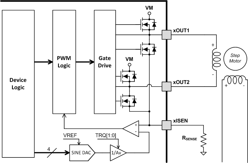
The PWM chopping current is set by a comparator which compares the voltage across a current sense resistor connected to the xISEN pin with a reference voltage. To generate the reference voltage for the current chopping comparator, the output of a sine lookup table is applied to a sine-weighted DAC, whose full-scale output voltage is set by VREF. This voltage is attenuated by a factor of Av. In addition, the TRQx pins further scale the reference.
 Figure 14. Current Regulation Block Diagram
 The full-scale (100%) chopping current is calculated as follows:

The TRQx pins are the inputs to a Torque DAC used to scale the output current. The current scalar value for different inputs is shown below.
Table 6. Torque DAC Settings
| TRQ1 | TRQ0 | CURRENT SCALAR (TRQ) | EFFECTIVE ATTENUATION |
|---|---|---|---|
| 1 | 1 | 25% | 26.4 V/V |
| 1 | 0 | 50% | 13.2 V/V |
| 0 | 1 | 75% | 8.8 V/V |
| 0 | 0 | 100% | 6.6 V/V |
Table 7 gives the xISEN trip voltage at a given DAC code and TRQ[1:0] setting for 1/16 step mode. In this table, VREF = 3.3 V.
Table 7. xISEN Trip Voltages over Torque DAC and Microsteps
| 1/16 STEP (SINE DAC CODE) | TORQUE DAC TRQ[1:0] SETTING | |||
|---|---|---|---|---|
| 00 – 100% | 01 – 75% | 10 – 50% | 11 – 25% | |
| 16 | 500.0 mV | 375.0 mV | 250.0 mV | 125.0 mV |
| 15 | 490.0 mV | 367.5 mV | 245.0 mV | 122.5 mV |
| 14 | 480.0 mV | 360.0 mV | 240.0 mV | 120.0 mV |
| 13 | 460.0 mV | 345.0 mV | 230.0 mV | 115.0 mV |
| 12 | 440.0 mV | 330.0 mV | 220.0 mV | 110.0 mV |
| 11 | 415.0 mV | 311.3 mV | 207.5 mV | 103.8 mV |
| 10 | 385.0 mV | 288.8 mV | 192.5 mV | 96.3 mV |
| 9 | 355.0 mV | 266.3 mV | 177.5 mV | 88.8 mV |
| 8 | 315.0 mV | 236.3 mV | 157.5 mV | 78.8 mV |
| 7 | 280.0 mV | 210.0 mV | 140.0 mV | 70.0 mV |
| 6 | 235.0 mV | 176.3 mV | 117.5 mV | 58.8 mV |
| 5 | 190.0 mV | 142.5 mV | 95.0 mV | 47.5 mV |
| 4 | 145.0 mV | 108.8 mV | 72.5 mV | 36.3 mV |
| 3 | 100.0 mV | 75.0 mV | 50.0 mV | 25.0 mV |
| 2 | 50.0 mV | 37.5 mV | 25.0 mV | 12.5 mV |
| 1 | 0.0 mV | 0.0 mV | 0.0 mV | 0.0 mV |