SLVSD18C June 2015 – August 2017 DRV8880
PRODUCTION DATA.
- 1 Features
- 2 Applications
- 3 Description
- 4 Revision History
- 5 Pin Configuration and Functions
- 6 Specifications
-
7 Detailed Description
- 7.1 Overview
- 7.2 Functional Block Diagram
- 7.3
Feature Description
- 7.3.1 Stepper Motor Driver Current Ratings
- 7.3.2 PWM Motor Drivers
- 7.3.3 Microstepping Indexer
- 7.3.4 Current Regulation
- 7.3.5
Decay Modes
- 7.3.5.1 Mode 1: Slow Decay for Increasing and Decreasing Current
- 7.3.5.2 Mode 2: Slow Decay for Increasing Current, Mixed Decay for Decreasing current
- 7.3.5.3 Mode 3: Mixed Decay for Increasing and Decreasing Current
- 7.3.5.4 Mode 4: Slow Decay for Increasing Current, Fast Decay for Decreasing current
- 7.3.5.5 Mode 5: Fast Decay for Increasing and Decreasing Current
- 7.3.6 Smart Tune
- 7.3.7 Adaptive Blanking Time
- 7.3.8 Charge Pump
- 7.3.9 LDO Voltage Regulator
- 7.3.10 Logic and Tri-Level Pin Diagrams
- 7.3.11 Power Supplies and Input Pins
- 7.3.12 Protection Circuits
- 7.3.13 VM UVLO (UVLO2)
- 7.3.14 Logic Undervoltage (UVLO1)
- 7.3.15 VCP Undervoltage Lockout (CPUV)
- 7.3.16 Thermal Shutdown (TSD)
- 7.3.17 Overcurrent Protection (OCP)
- 7.4 Device Functional Modes
- 8 Application and Implementation
- 9 Power Supply Recommendations
- 10Layout
- 11Device and Documentation Support
- 12Mechanical, Packaging, and Orderable Information
パッケージ・オプション
デバイスごとのパッケージ図は、PDF版データシートをご参照ください。
メカニカル・データ(パッケージ|ピン)
- RHR|28
- PWP|28
サーマルパッド・メカニカル・データ
発注情報
7.3.17 Overcurrent Protection (OCP)
An analog current limit circuit on each FET limits the current through the FET by removing the gate drive. If this analog current limit persists for longer than tOCP, all FETs in the H-bridge will be disabled and nFAULT will be driven low. In addition to this FET current limit, an overcurrent condition is also detected if the voltage at xISEN exceeds VOCP.
The overcurrent fault response can be set to either latched mode or retry mode:
 Figure 25. Latched OCP Mode
  Figure 26. Retry OCP Mode
 In latched mode, operation will resume after the ENABLE pin is brought logic low for at least 1 μs to reset the output driver. The nFAULT pin will be released after ENABLE is returned logic high. Removing and re-applying VM or toggling nSLEEP will also reset the latched fault.
In retry mode, the driver will be re-enabled after the OCP retry period (tRETRY) has passed. nFAULT becomes high again after the retry time. If the fault condition is still present, the cycle repeats. If the fault is no longer present, normal operation resumes and nFAULT remains deasserted.
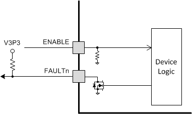
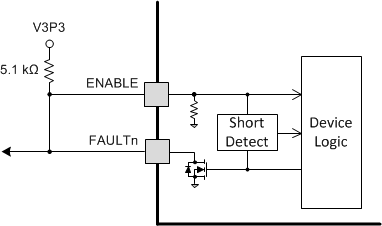
A microcontroller can retain control of the ENABLE pin while in retry mode if it is operated like an open-drain output. Many microcontrollers support this. When the DRV8880 is operating normally, configure the MCU GPIO as an input. In this state, the MCU can detect whenever nFAULT is pulled low. In order to disable the DRV8880 output, configure the GPIO output state as low, and then configure the GPIO as an output.
Alternatively, a logic-level FET may be used to create an open drain external to the MCU. In this case, an additional MCU GPIO may be required in order to monitor the nFAULT pin.
 Figure 27. Methods For Operating in Retry Mode
 Table 10. Fault Condition Summary
| FAULT | CONDITION | ERROR REPORT | H-BRIDGE | CHARGE PUMP | INDEXER | V3P3 | RECOVERY |
|---|---|---|---|---|---|---|---|
| VM undervoltage
(UVLO2) |
VM < VUVLO2
(max 6.4 V) |
nFAULT | Disabled | Disabled | Operating |
Operating |
VM > VUVLO2
(max 6.5 V) |
| Logic undervoltage
(UVLO1) |
VM < VUVLO2
(max 4.9 V) |
None | Disabled | Disabled | Disabled |
Operating |
VM > VUVLO2
(max 4.8 V) |
| VCP undervoltage
(CPUV) |
VCP < VCPUV
(typ VM + 1.8 V) |
nFAULT | Disabled | Operating | Operating |
Operating |
VCP > VCPUV
(typ VM + 1.9 V) |
| Thermal Shutdown
(TSD) |
TJ > TTSD
(min 150°C) |
nFAULT | Disabled | Operating | Operating |
Operating |
TJ < TTSD - THYS
(THYS typ 35°C) |
| Overcurrent
(OCP) |
IOUT > IOCP
(min 2.5 A) VxISEN > VOCP (min 0.9 V) |
nFAULT | Disabled | Operating | Operating |
Operating |
ENABLE
-or- tRETRY |