SLVSD18C June 2015 – August 2017 DRV8880
PRODUCTION DATA.
- 1 Features
- 2 Applications
- 3 Description
- 4 Revision History
- 5 Pin Configuration and Functions
- 6 Specifications
-
7 Detailed Description
- 7.1 Overview
- 7.2 Functional Block Diagram
- 7.3
Feature Description
- 7.3.1 Stepper Motor Driver Current Ratings
- 7.3.2 PWM Motor Drivers
- 7.3.3 Microstepping Indexer
- 7.3.4 Current Regulation
- 7.3.5
Decay Modes
- 7.3.5.1 Mode 1: Slow Decay for Increasing and Decreasing Current
- 7.3.5.2 Mode 2: Slow Decay for Increasing Current, Mixed Decay for Decreasing current
- 7.3.5.3 Mode 3: Mixed Decay for Increasing and Decreasing Current
- 7.3.5.4 Mode 4: Slow Decay for Increasing Current, Fast Decay for Decreasing current
- 7.3.5.5 Mode 5: Fast Decay for Increasing and Decreasing Current
- 7.3.6 Smart Tune
- 7.3.7 Adaptive Blanking Time
- 7.3.8 Charge Pump
- 7.3.9 LDO Voltage Regulator
- 7.3.10 Logic and Tri-Level Pin Diagrams
- 7.3.11 Power Supplies and Input Pins
- 7.3.12 Protection Circuits
- 7.3.13 VM UVLO (UVLO2)
- 7.3.14 Logic Undervoltage (UVLO1)
- 7.3.15 VCP Undervoltage Lockout (CPUV)
- 7.3.16 Thermal Shutdown (TSD)
- 7.3.17 Overcurrent Protection (OCP)
- 7.4 Device Functional Modes
- 8 Application and Implementation
- 9 Power Supply Recommendations
- 10Layout
- 11Device and Documentation Support
- 12Mechanical, Packaging, and Orderable Information
パッケージ・オプション
デバイスごとのパッケージ図は、PDF版データシートをご参照ください。
メカニカル・データ(パッケージ|ピン)
- RHR|28
- PWP|28
サーマルパッド・メカニカル・データ
発注情報
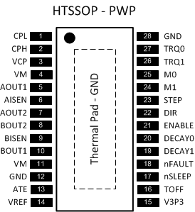
5 Pin Configuration and Functions
PWP PowerPAD™ Package
28-Pin HTSSOP
Top View

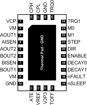
RHR Package
28-Pin WQFN With Exposed Thermal Pad
Top View

Pin Functions
| PIN | TYPE | DESCRIPTION | |||
|---|---|---|---|---|---|
| NAME | PWP | RHR | |||
| CPL | 1 | 27 | PWR | Charge pump switching pins | Connect a VM rated, 0.1-µF ceramic capacitor between CPH and CPL |
| CPH | 2 | 28 | |||
| VCP | 3 | 1 | O | Charge pump output | Connect a 16 V, 0.47 µF ceramic capacitor to VM |
| VM | 4, 11 | 2, 9 | PWR | Power supply | Connect to motor supply voltage; bypass to GND with two 0.1 µF (for each pin) plus one bulk capacitor rated for VM |
| AOUT1 | 5 | 3 | O | Winding A output | H-bridge outputs, drives one winding of a stepper motor |
| AOUT2 | 7 | 5 | |||
| AISEN | 6 | 4 | O | Winding A sense | Requires sense resistor to GND; value sets peak current in winding A |
| BOUT2 | 8 | 6 | O | Winding B output | H-bridge outputs, drives one winding of a stepper motor |
| BOUT1 | 10 | 8 | |||
| BISEN | 9 | 7 | O | Winding B sense | Requires sense resistor to GND; value sets peak current in winding B |
| GND | 12, 28 | 10, 26 | PWR | Device ground | Must be connected to ground |
| ATE | 13 | 11 | I | Smart tune enable pin | Logic high enables smart tune operation; when logic low, the decay mode is set through the DECAYx pins; smart tune must be pulled high prior to power-up or coming out of sleep, or else tied to V3P3 in order to enable smart tune; internal pulldown; see Smart Tune |
| VREF | 14 | 12 | I | Full scale current reference input | Voltage on this pin sets the full scale chopping current. |
| V3P3 | 15 | 13 | PWR | Internal regulator | Internal supply voltage; bypass to GND with a 6.3 V, 0.47 µF ceramic capacitor; up to 10 mA external load |
| TOFF | 16 | 14 | I | Decay mode off time set | Sets the off-time during current chopping; tri-level pin |
| nSLEEP | 17 | 15 | I | Sleep mode input | Logic high to enable device; logic low to enter low-power sleep mode; internal pulldown |
| nFAULT | 18 | 16 | O | Fault indication pin | Pulled logic low with fault condition; open-drain output requires an external pullup |
| DECAY1 | 19 | 17 | I | Decay mode setting pins | Sets the decay mode; see description section; tri-level pin |
| DECAY0 | 20 | 18 | |||
| ENABLE | 21 | 19 | I | Enable driver input | Logic high to enable device outputs and internal indexer; logic low to disable; internal pulldown |
| DIR | 22 | 20 | I | Direction input | Logic level sets the direction of stepping; internal pulldown |
| STEP | 23 | 21 | I | Step input | A rising edge causes the indexer to advance one step; internal pulldown |
| M1 | 24 | 22 | I | Microstepping mode setting pins | Sets the step mode; full, 1/2, 1/4, 1/8, 1/16; tri-level pin |
| M0 | 25 | 23 | |||
| TRQ1 | 26 | 24 | I | Torque DAC current scalar | Scales the current by 100%, 75%, 50%, or 25%; internal pulldown |
| TRQ0 | 27 | 25 | |||
| PAD | PAD | PAD | PWR | Thermal pad | Must be connected to ground |