JAJSCW7D January 2016 – November 2018 DRV8884
PRODUCTION DATA.
- 1 特長
- 2 アプリケーション
- 3 概要
- 4 改訂履歴
- 5 概要(続き)
- 6 Pin Configuration and Functions
- 7 Specifications
-
8 Detailed Description
- 8.1 Overview
- 8.2 Functional Block Diagram
- 8.3
Feature Description
- 8.3.1 Stepper Motor Driver Current Ratings
- 8.3.2 PWM Motor Drivers
- 8.3.3 Microstepping Indexer
- 8.3.4 Current Regulation
- 8.3.5 Controlling RREF With an MCU DAC
- 8.3.6 Decay Modes
- 8.3.7 Blanking Time
- 8.3.8 Charge Pump
- 8.3.9 LDO Voltage Regulator
- 8.3.10 Logic and Multi-Level Pin Diagrams
- 8.3.11 Protection Circuits
- 8.4 Device Functional Modes
- 9 Application and Implementation
- 10Power Supply Recommendations
- 11Layout
- 12デバイスおよびドキュメントのサポート
- 13メカニカル、パッケージ、および注文情報
パッケージ・オプション
メカニカル・データ(パッケージ|ピン)
サーマルパッド・メカニカル・データ
発注情報
8.3.9 LDO Voltage Regulator
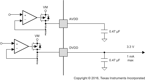
An LDO regulator is integrated into the DRV8884. DVDD can be used to provide a reference voltage. For proper operation, bypass DVDD to GND using a ceramic capacitor.
The DVDD output is nominally 3.3 V. When the DVDD LDO current load exceeds 1 mA, the output voltage drops significantly.
The AVDD pin also requires a bypass capacitor to GND. This LDO is for DRV8884 internal use only.
 Figure 22. LDO Diagram
 If a digital input needs to be tied permanently high (that is, Mx, DECAY, or TRQ), it is preferable to tie the input to DVDD instead of an external regulator. This saves power when VM is not applied or in sleep mode; DVDD is disabled and current will not be flowing through the input pulldown resistors. For reference, logic level inputs have a typical pulldown of 100 kΩ, and tri-level inputs have a typical pulldown of 60 kΩ.