SNLS338F January 2011 – November 2014 DS100BR111
PRODUCTION DATA.
- 1 Features
- 2 Applications
- 3 Description
- 4 Simplified Schematic
- 5 Revision History
- 6 Pin Configuration and Functions
- 7 Specifications
- 8 Detailed Description
- 9 Application and Implementation
- 10Power Supply Recommendations
- 11Layout
- 12Device and Documentation Support
- 13Mechanical, Packaging, and Orderable Information
パッケージ・オプション
メカニカル・データ(パッケージ|ピン)
- RTW|24
サーマルパッド・メカニカル・データ
- RTW|24
発注情報
8 Detailed Description
8.1 Overview
The DS100BR111 is a high performance bidirectional 1-lane repeater optimized for 10G-KR and SAS/SATA operation, where its programmable equalization and de-emphasis compensate for lossy FR-4 printed circuit board backplanes or balanced cables. The DS100BR111 operates in 3 modes: Pin Control Mode (ENSMB = 0), SMBus Slave Mode (ENSMB = 1), and SMBus Master Mode (ENSMB = Float) to load register information from external EEPROM.
Each channel has a signal detector circuit that monitors the input signal amplitude. When the input signal level is below the detector's de-assert level, the output is disabled. When input signal level exceeds the detector's assert level, the output is enabled. The signal detector circuit is used to support the OOB signaling used in SAS and SATA.
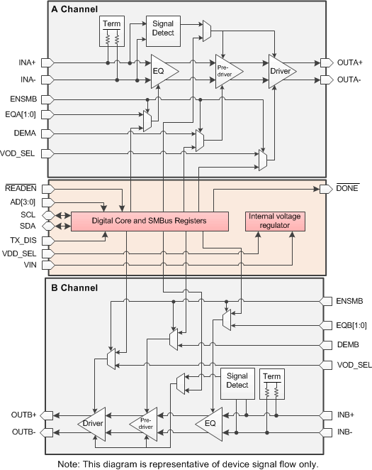
8.2 Functional Block Diagram
8.3 Feature Description
8.3.1 4-Level Control Pin Settings
The 4-level input pins use a resistor divider to set the four valid control levels and provide a wider range of control settings when ENSMB = 0. There is an internal 30-kΩ pull-up and a 60-kΩ pull-down connected to the package pin. These resistors, together with the external resistor connection, combine to achieve the desired voltage level. By using the 1-kΩ pull-down, 20-kΩ pull-down, no connect, or 1-kΩ pull-up, the optimal voltage levels for each of the four input states are achieved as shown in Table 1.
Table 1. 4–Level Control Pin Settings Table
| RESULTING PIN VOLTAGE | |||
|---|---|---|---|
| LEVEL | SETTING | 3.3 V MODE | 2.5 V MODE |
| 0 | Tie 1 kΩ to GND | 0.10 V | 0.08 V |
| R | Tie 20 kΩ to GND | 1/3 x VIN | 1/3 x VDD |
| F | Float (leave pin open) | 2/3 x VIN | 2/3 x VDD |
| 1 | Tie 1 kΩ to VIN or VDD | VIN - 0.05 V | VDD - 0.04 V |
Typical 4-Level Input Thresholds:
- Internal Threshold between 0 and R = 0.2 * VIN or VDD
- Internal Threshold between R and F = 0.5 * VIN or VDD
- Internal Threshold between F and 1 = 0.8 * VIN or VDD
In order to minimize the startup current associated with the integrated 2.5-V regulator, the 1-kΩ pull-up / pull-down resistors are recommended. If several four level inputs require the same setting, it is possible to combine two or more 1-kΩ resistors into a single lower value resistor. As an example, combining two inputs with a single 500-Ω resistor is a valid way to save board space.
8.4 Device Functional Modes
8.4.1 Pin Control Mode
When in Pin Mode (ENSMB = 0), equalization, de-emphasis, and VOD (output amplitude) can be selected via external pin control for both the A-channel and B-channel. Equalization and de-emphasis can be programmed by pin selection for each side independently. For further device control, the VOD_SEL and MODE pins are available to improve DS100BR111 performance depending on design applications. The receiver electrical idle detect threshold is also adjustable via the SD_TH pin. Pin control mode is ideal in situations where neither MCU or EEPROM is available to access the device via SMBus SDA and SCL lines.
8.4.2 SMBus Slave Mode
When in Slave SMBus Mode (ENSMB = 1), equalization, de-emphasis, and VOD (output amplitude) are all programmable on an individual channel basis. Upon assertion of ENSMB, the EQx, DEMx, and VODx settings are controlled by SMBus immediately. It is important to note that SMBus settings can only be changed from their defaults after asserting Register Enable by setting Reg 0x06[3] = 1. The EQx, DEMx, and VODx pins are subsequently converted to AD0-AD3 SMBus address inputs. The other external control pins (TX_DIS, MODE, and SD_TH) remain active unless their respective registers are written to and the appropriate override bit is set. If the user overrides a pin control, the input voltage level of that control pin is ignored until ENSMB is driven low (Pin Mode). In the event that channels are powered down via the TX_DIS pin, register setting states are not affected.
Table 2. Signal Detect Threshold Level(1)
| LEVEL | SD_TH (Pin 14) | SMBus REG BIT [3:2] and [1:0] | TYPICAL ASSERT LEVEL (mVpp) | TYPICAL DE-ASSERT LEVEL (mVpp) |
|---|---|---|---|---|
| 1 | 0 | 10 | 210 | 150 |
| 2 | R | 01 | 160 | 100 |
| 3 | F (Default) | 00 | 180 | 110 |
| 4 | 1 | 11 | 190 | 130 |
8.4.3 SMBus Master Mode
When in SMBus Master Mode (ENSMB = Float), the equalization, de-emphasis, and VOD (output amplitude) for multiple devices can be loaded via external EEPROM. By asserting a Float condition on the ENSMB pin, an external EEPROM writes register settings to each device in accordance with its SMBus slave address. The settings programmable by external EEPROM provide only a subset of all the register bits available via SMBus Slave Mode, and the bit-mapping between SMBus Slave Mode registers and EEPROM addresses can be referenced in Table 6. Once the EEPROM successfully finishes loading each device's register settings, the device reverts back to SMBus Slave Mode and releases SDA and SCL control to an external master MCU. If the EEPROM fails to load settings to a particular device, for example due to an invalid or blank hex file, the device waits indefinitely in an unknown state where access to the SMBus lines is not possible.
8.4.4 Signal Conditioning Settings
Equalization, de-emphasis, and VOD settings accessible via the pin controls are chosen to meet the needs of most high speed applications. For additional levels and flexibility in EQ, de-emphasis, and VOD programming, these settings can be controlled via the SMBus registers. Each control pin input has a total of four possible voltage level settings. In pin mode, Table 3 shows the 16 EQ settings available, and Table 4 shows the 16 de-emphasis and VOD combination settings available. Note that when in pin mode, only 16 of a possible 256 EQ programmable levels can be accessed by setting the EQx[1:0] pins. In addition, each pin setting applied to the VOD_SEL and DEMx pin input programs a fixed combination of VOD and de-emphasis. In order to access all 256 EQ levels and control both VOD and de-emphasis settings independently, SMBus register access must be used.
Table 3. Equalizer Settings
| EQUALIZATION BOOST RELATIVE TO DC | |||||
|---|---|---|---|---|---|
| LEVEL | EQA1
EQB1 |
EQA0
EQB0 |
EQ — 8 bits [7:0] | dB BOOST at 5 GHz | SUGGESTED MEDIA(1) |
| 1 | 0 | 0 | 0000 0000 = 0x00 | 2.5 | FR4 < 5 inch trace |
| 2 | 0 | R | 0000 0001 = 0x01 | 6.5 | FR4 5 inch trace |
| 3 | 0 | F | 0000 0010 = 0x02 | 9 | FR4 10 inch trace |
| 4 | 0 | 1 | 0000 0011 = 0x03 | 11.5 | FR4 15 inch trace |
| 5 | R | 0 | 0000 0111 = 0x07 | 14 | FR4 20 inch trace |
| 6 | R | R | 0001 0101 = 0x15 | 15 | FR4 25 inch trace |
| 7 | R | F | 0000 1011 = 0x0B | 17 | FR4 25 inch trace |
| 8 | R | 1 | 0000 1111 = 0x0F | 19 | 7m 30 AWG Cable |
| 9 | F | 0 | 0101 0101 = 0x55 | 20 | FR4 30 inch trace |
| 10 | F | R | 0001 1111 = 0x1F | 23 | 8m 30 AWG Cable FR4 35 inch trace |
| 11 | F | F | 0010 1111 = 0x2F | 25 | 10m 30 AWG Cable |
| 12 | F | 1 | 0011 1111 = 0x3F | 27 | 10m to 12m, Cable |
| 13 | 1 | 0 | 1010 1010 = 0xAA | 30 | |
| 14 | 1 | R | 0111 1111 = 0x7F | 31 | |
| 15 | 1 | F | 1011 1111 = 0xBF | 33 | |
| 16 | 1 | 1 | 1111 1111 = 0xFF | 34 | |
Table 4. De-Emphasis and Output Voltage Settings(1)
| LEVEL | VOD_SEL(2)(3) | DEMA/B | SMBus REGISTER
DEM Level |
SMBus REGISTER
VOD LEVEL |
VOD (mVpp) | DEM (dB) |
|---|---|---|---|---|---|---|
| 1 | 0 | 0 | 000 | 000 | 700 | 0 |
| 2 | 0 | F | 010 | 000 | 700 | -3.5 |
| 3 | 0 | R | 011 | 000 | 700 | -6 |
| 4 | 0 | 1 | 101 | 000 | 700 | -9 |
| 5 | F | 0 | 000 | 011 | 1000 | 0 |
| 6 | F | F | 010 | 011 | 1000 | -3.5 |
| 7 | F | R | 011 | 011 | 1000 | -6 |
| 8 | F | 1 | 101 | 011 | 1000 | -9 |
| 9 | R | 0 | 000 | 101 | 1200 | -0 |
| 10 | R | F | 010 | 101 | 1200 | -3.5 |
| 11 | R | R | 011 | 101 | 1200 | -6 |
| 12 | R | 1 | 101 | 101 | 1200 | -9 |
| 13 | 1 | 0 | 000 | 100 | 1100 | 0 |
| 14 | 1 | F | 001 | 100 | 1100 | -1.5 |
| 15 | 1 | R | 001 | 110 | 1300 | -1.5 |
| 16 | 1 | 1 | 010 | 110 | 1300 | -3.5 |
8.5 Programming
8.5.1 System Management Bus (SMBus) and Configuration Registers
The System Management Bus interface is compatible with the SMBus 2.0 physical layer specification. Tie ENSMB = 1 kΩ to VDD (2.5 V mode) or VIN (3.3 V mode) to enable SMBus Slave Mode and allow access to the configuration registers.
The DS100BR111 uses AD[3:0] inputs in both SMBus Modes. These AD[3:0] pins are the user set SMBus slave address inputs and have internal pull-downs. Based on the SMBus 2.0 specification, the DS100BR111 has a 7-bit slave address. The LSB is set to 0'b (for a WRITE). When AD[3:0] pins are left floating or pulled low, AD[3:0] = 0000'b, and the device default address byte is 0xB0. The device supports up to 16 address bytes, as shown in Table 5.
Table 5. Device Slave Address Bytes
| AD[3:0] SETTINGS | FULL SLAVE ADDRESS BYTE (7-Bit ADDRESS + WRITE BIT) |
7-Bit SLAVE ADDRESS (HEX) |
|---|---|---|
| 0000 | B0 | 58 |
| 0001 | B2 | 59 |
| 0010 | B4 | 5A |
| 0011 | B6 | 5B |
| 0100 | B8 | 5C |
| 0101 | BA | 5D |
| 0110 | BC | 5E |
| 0111 | BE | 5F |
| 1000 | C0 | 60 |
| 1001 | C2 | 61 |
| 1010 | C4 | 62 |
| 1011 | C6 | 63 |
| 1100 | C8 | 64 |
| 1101 | CA | 65 |
| 1110 | CC | 66 |
| 1111 | CE | 67 |
The SDA and SCL pins are 3.3 V tolerant, but are not 5 V tolerant. An external pull-up resistor is required on the SDA and SCL line. The resistor value can be from 2 kΩ to 5 kΩ depending on the voltage, loading, and speed.
8.5.2 Transfer Of Data Via the SMBus
During normal operation, the data on SDA must be stable during the time when SCL is High.
There are three unique states for the SMBus:
- START: A High-to-Low transition on SDA while SCL is High indicates a message START condition.
- STOP: A Low-to-High transition on SDA while SCL is High indicates a message STOP condition.
- IDLE: If SCL and SDA are both High for a time exceeding tBUF from the last detected STOP condition or if they are High for a total exceeding the maximum specification for tHIGH, then the bus will transfer to the IDLE state.
8.5.3 SMBus Transactions
The device supports WRITE and READ transactions. See Table 9 for register address, type (Read/Write, Read Only), default value, and function information.
8.5.4 Writing a Register
To write a register, the following protocol is used (see SMBus 2.0 specification):
- The Host drives a START condition, the 7-bit SMBus address, and a “0” indicating a WRITE.
- The Device (Slave) drives the ACK bit (“0”).
- The Host drives the 8-bit Register Address.
- The Device drives an ACK bit (“0”).
- The Host drive the 8-bit data byte.
- The Device drives an ACK bit (“0”).
- The Host drives a STOP condition.
Once the WRITE transaction is completed, the bus goes IDLE and communication with other SMBus devices may now occur.
8.5.5 Reading a Register
To read a register, the following protocol is used (see SMBus 2.0 specification):
- The Host drives a START condition, the 7-bit SMBus address, and a “0” indicating a WRITE.
- The Device (Slave) drives the ACK bit (“0”).
- The Host drives the 8-bit Register Address.
- The Device drives an ACK bit (“0”).
- The Host drives a START condition.
- The Host drives the 7-bit SMBus Address, and a “1” indicating a READ.
- The Device drives an ACK bit “0”.
- The Device drives the 8-bit data value (register contents).
- The Host drives a NACK bit “1”indicating end of the READ transfer.
- The Host drives a STOP condition.
Once the READ transaction is completed, the bus goes IDLE and communication with other SMBus devices may now occur.
Please see Table 9 for more information.
8.5.6 EEPROM Programming
The DS100BR111 supports reading directly from an external EEPROM device by implementing SMBus Master mode. When used in SMBus Master mode, the DS100BR111 will read directly from a specific location in the external EEPROM. When designing a system that uses external EEPROM, the following guidelines should be followed:
- Set the DS100BR111 in SMBus Master Mode.
- ENSMB (Pin 3) = Float
- The external EEPROM device must support 1 MHz operation.
- The external EEPROM device address byte must be 0xA0.
- Set the AD[3:0] inputs for SMBus address byte. When AD[3:0] = 0000'b, the device address byte is 0xB0.
- The device address can be set with the use of the AD[3:0] input up to 16 different addresses. Use the example below to set each of the SMBus addresses.
- AD[3:0] = 0001'b, the device address byte is 0xB2
- AD[3:0] = 0010'b, the device address byte is 0xB4
- AD[3:0] = 0011'b, the device address byte is 0xB6
- AD[3:0] = 0100'b, the device address byte is 0xB8
- The master implementation in the DS100BR111 supports multiple devices reading from one EEPROM. When tying multiple devices to the SDA and SCL pins, use these guidelines:
- Use adjacent SMBus addresses for the 4 devices
- Use a pull-up resistor on SDA; value = 4.7 kΩ
- Use a pull-up resistor on SCL: value = 4.7 kΩ
- Daisy-chain READEN (Pin 17) and DONE (Pin 18) from one device to the next device in the sequence.
- Tie READEN of the 1st device in the chain (U1) to GND
- Tie DONE of U1 to READEN of U2
- Tie DONE of U2 to READEN of U3
- Tie DONE of U3 to READEN of U4
- Optional: Tie DONE of U4 to a LED to show each of the devices have been loaded successfully
8.5.6.1 Master EEPROM Programming
Below is an example of a 2 kbits (256 x 8-bit) EEPROM in hex format for the DS100BR111 device. The first 3 bytes of the EEPROM always contain a header common and necessary to control initialization of all devices connected to the same SMBus line. There is a CRC enable flag to enable or disable CRC checking. There is a MAP bit to flag the presence of an address map that specifies the configuration data start address in the EEPROM. If the MAP bit is not present, the configuration data start address immediately follows the 3-byte base header. A bit to indicate an EEPROM size > 256 bytes is necessary to address the EEPROM properly. There are 37 bytes of data size for each DS100BR111 device. For more details about EEPROM programming and Master mode, refer to SNLA228.
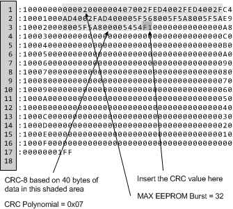 Figure 8. Typical EEPROM Data Set
NOTE
The maximum EEPROM size supported is 8 kbits (1024 x 8 bits).
The CRC-8 calculation is performed for each device on the first 3 bytes of header information plus the 37 bytes of data for the DS100BR111 or 40 bytes in total. The result of this calculation is placed immediately after the DS100BR111 data in the EEPROM which ends with "5454". The CRC-8 in the DS100BR111 uses a polynomial = x8 + x2 + x + 1.
There are two pins that provide unique functions in SMBus Master mode:
- DONE
- READEN
When the DS100BR111 is powered up in SMBus Master mode, it reads its configuration from the external EEPROM when the READEN pin goes low. When the DS100BR111 is finished reading its configuration from the external EEPROM, it drives the DONE pin low. In applications where there is more than one DS100BR111 on the same SMBus, bus contention can result if more than one DS100BR111 tries to take control of the SMBus at the same time. The READEN and DONE pins prevent this bus contention. The system should be designed so that the READEN pin from one DS100BR111 in the system is driven low on power-up. This DS100BR111 will take command of the SMBus on power-up and will read its initial configuration from the external EEPROM. When the first DS100BR111 is finished reading its configuration, it will drive the DONE pin low. This pin should be connected to the READEN pin of another DS100BR111. When this second DS100BR111 senses its READEN pin driven low, it will take command of the SMBus and read its initial configuration from the external EEPROM, after which it will set its DONE pin low. By connecting the DONE pin of each DS100BR111 to the READEN pin of the next DS100BR111, each DS100BR111 can read its initial configuration from the EEPROM without causing bus contention.
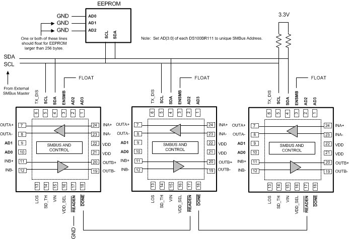 Figure 9. Typical Multi-device EEPROM Connection Diagram
8.5.6.2 EEPROM Address Mapping
A detailed EEPROM Address Mapping for a single device is shown in Table 6. For instances where multiple devices are written to EEPROM, the device starting address definitions align starting with Byte 0x03. A register map overview for a multi-device EEPROM address map is shown in Table 7.
Table 6. Single Device with Default Value
| EEPROM Address Byte | BIT 7 | BIT 6 | BIT 5 | BIT 4 | BIT 3 | BIT 2 | BIT 1 | BIT 0 | ||
|---|---|---|---|---|---|---|---|---|---|---|
| Description | 0x00 | CRC_EN | Address Map Present | EEPROM > 256 Bytes | Reserved | DEVICE COUNT[3] | DEVICE COUNT[2] | DEVICE COUNT[1] | DEVICE COUNT[0] | |
| Default Value | 0x00 | 0 | 0 | 0 | 0 | 0 | 0 | 0 | 0 | |
| Description | 0x01 | Reserved | Reserved | Reserved | Reserved | Reserved | Reserved | Reserved | Reserved | |
| Default Value | 0x00 | 0 | 0 | 0 | 0 | 0 | 0 | 0 | 0 | |
| Description | 0x02 | Max EEPROM Burst size[7] | Max EEPROM Burst size[6] | Max EEPROM Burst size[5] | Max EEPROM Burst size[4] | Max EEPROM Burst size[3] | Max EEPROM Burst size[2] | Max EEPROM Burst size[1] | Max EEPROM Burst size[0] | |
| Default Value | 0x00 | 0 | 0 | 0 | 0 | 0 | 0 | 0 | 0 | |
| Description | 0x03 | Cont_talk_EN_CHA | Cont_talk_EN_CHB | Reserved | Reserved | Reserved | Sel_LOS | Reserved | Reserved | |
| SMBus Register | 0x01[7] | 0x01[6] | 0x01[5] | 0x01[4] | 0x01[3] | 0x01[2] | 0x01[1] | 0x01[0] | ||
| Default Value | 0x00 | 0 | 0 | 0 | 0 | 0 | 0 | 0 | 0 | |
| Description | 0x04 | Ovrd_LOS | LOS_Value | PWDN_Inputs | PWDN_Osc | Reserved | eSATA En CHA | eSATA En CHB | Ovrd TX_DIS | |
| SMBus Register | 0x02[5] | 0x02[4] | 0x02[3] | 0x02[2] | 0x02[0] | 0x04[7] | 0x04[6] | 0x04[5] | ||
| Default Value | 0x00 | 0 | 0 | 0 | 0 | 0 | 0 | 0 | 0 | |
| Description | 0x05 | TX_DIS CHA | TX_DIS CHB | Reserved | EQ Stage 4 CHB | EQ Stage 4 CHA | Reserved | Ovrd IDLE_TH | Reserved | |
| SMBus Register | 0x04[4] | 0x04[3] | 0x04[2] | 0x04[1] | 0x04[0] | 0x06[4] | 0x08[6] | 0x08[5] | ||
| Default Value | 0x04 | 0 | 0 | 0 | 0 | 0 | 1 | 0 | 0 | |
| Description | 0x06 | Ovrd IDLE | Reserved | Ovrd Out_Mode | Ovrd DEM | Reserved | Reserved | Reserved | Reserved | |
| SMBus Register | 0x08[4] | 0x08[3] | 0x08[2] | 0x08[1] | 0x08[0] | 0x0B[6] | 0x0B[5] | 0x0B[4] | ||
| Default Value | 0x07 | 0 | 0 | 0 | 0 | 0 | 1 | 1 | 1 | |
| Description | 0x07 | Reserved | Reserved | Reserved | Reserved | CHA_Idle_Auto | CHA_Idle_Sel | Reserved | Reserved | |
| SMBus Register | 0x0B[3] | 0x0B[2] | 0x0B[1] | 0x0B[0] | 0x0E[5] | 0x0E[4] | 0x0E[3] | 0x0E[2] | ||
| Default Value | 0x00 | 0 | 0 | 0 | 0 | 0 | 0 | 0 | 0 | |
| Description | 0x08 | CHA_EQ[7] | CHA_EQ[6] | CHA_EQ[5] | CHA_EQ[4] | CHA_EQ[3] | CHA_EQ[2] | CH0_EQ[1] | CH0_EQ[0] | |
| SMBus Register | 0x0F[7] | 0x0F[6] | 0x0F[5] | 0x0F[4] | 0x0F[3] | 0x0F[2] | 0x0F[1] | 0x0F[0] | ||
| Default Value | 0x2F | 0 | 0 | 1 | 0 | 1 | 1 | 1 | 1 | |
| Description | 0x09 | CHA_Sel SCP | CHA_Out Mode | Reserved | Reserved | Reserved | Reserved | Reserved | Reserved | |
| SMBus Register | 0x10[7] | 0x10[6] | 0x10[5] | 0x10[4] | 0x10[3] | 0x10[2] | 0x10[1] | 0x10[0] | ||
| Default Value | 0xED | 1 | 1 | 1 | 0 | 1 | 1 | 0 | 1 | |
| Description | 0x0A | CHA_DEM[2] | CHA_DEM[1] | CHA_DEM[0] | Reserved | CHA_Idle_ThA[1] | CHA_Idle_ThA[0] | CHA_Idle_ThD[1] | CHA_Idle_ThD[0] | |
| SMBus Register | 0x11[2] | 0x11[1] | 0x11[0] | 0x12[7] | 0x12[3] | 0x12[2] | 0x12[1] | 0x12[0] | ||
| Default Value | 0x40 | 0 | 1 | 0 | 0 | 0 | 0 | 0 | 0 | |
| Description | 0x0B | CHB_Idle_Auto | CHB_Idle_Sel | Reserved | Reserved | CHB_EQ[7] | CHB_EQ[6] | CHB_EQ[5] | CHB_EQ[4] | |
| SMBus Register | 0x15[5] | 0x15[4] | 0x15[3] | 0x15[2] | 0x16[7] | 0x16[6] | 0x16[5] | 0x16[4] | ||
| Default Value | 0x02 | 0 | 0 | 0 | 0 | 0 | 0 | 1 | 0 | |
| Description | 0x0C | CHB_EQ[3] | CHB_EQ[2] | CHB_EQ[1] | CHB_EQ[0] | CHB_Sel SCP | CHB_Out Mode | Reserved | Reserved | |
| SMBus Register | 0x16[3] | 0x16[2] | 0x16[1] | 0x16[0] | 0x17[7] | 0x17[6] | 0x17[5] | 0x17[4] | ||
| Default Value | 0xFE | 1 | 1 | 1 | 1 | 1 | 1 | 1 | 0 | |
| Description | 0x0D | Reserved | Reserved | Reserved | Reserved | CHB_DEM[2] | CHB_DEM[1] | CHB_DEM[0] | Reserved | |
| SMBus Register | 0x17[3] | 0x17[2] | 0x17[1] | 0x17[0] | 0x18[2] | 0x18[1] | 0x18[0] | 0x19[7] | ||
| Default Value | 0xD4 | 1 | 1 | 0 | 1 | 0 | 1 | 0 | 0 | |
| Description | 0x0E | CHB_Idle_ThA[1] | CHB_Idle_ThA[0] | CHB_Idle_ThD[1] | CHB_Idle_ThD[0] | Reserved | Reserved | Reserved | Reserved | |
| SMBus Register | 0x19[3] | 0x19[2] | 0x19[1] | 0x19[0] | 0x1C[5] | 0x1C[4] | 0x1C[3] | 0x1C[2] | ||
| Default Value | 0x00 | 0 | 0 | 0 | 0 | 0 | 0 | 0 | 0 | |
| Description | 0x0F | Reserved | Reserved | Reserved | Reserved | Reserved | Reserved | Reserved | Reserved | |
| SMBus Register | 0x1D[7] | 0x1D[6] | 0x1D[5] | 0x1D[4] | 0x1D[3] | 0x1D[2] | 0x1D[1] | 0x1D[0] | ||
| Default Value | 0x2F | 0 | 0 | 1 | 0 | 1 | 1 | 1 | 1 | |
| Description | 0x10 | Reserved | Reserved | Reserved | Reserved | Reserved | Reserved | Reserved | Reserved | |
| SMBus Register | 0x1E[7] | 0x1E[6] | 0x1E[5] | 0x1E[4] | 0x1E[3] | 0x1E[2] | 0x1E[1] | 0x1E[0] | ||
| Default Value | 0xAD | 1 | 0 | 1 | 0 | 1 | 1 | 0 | 1 | |
| Description | 0x11 | Reserved | Reserved | Reserved | Reserved | Reserved | Reserved | Reserved | Reserved | |
| SMBus Register | 0x1F[2] | 0x1F[1] | 0x1F[0] | 0x20[7] | 0x20[3] | 0x20[2] | 0x20[1] | 0x20[0] | ||
| Default Value | 0x40 | 0 | 1 | 0 | 0 | 0 | 0 | 0 | 0 | |
| Description | 0x12 | Reserved | CHA_VOD[2] | CHA_VOD[1] | CHA_VOD[0] | Reserved | Reserved | Reserved | Reserved | |
| SMBus Register | 0x23[5] | 0x23[4] | 0x23[3] | 0x23[2] | 0x24[7] | 0x24[6] | 0x24[5] | 0x24[4] | ||
| Default Value | 0x02 | 0 | 0 | 0 | 0 | 0 | 0 | 1 | 0 | |
| Description | 0x13 | Reserved | Reserved | Reserved | Reserved | Reserved | Reserved | Reserved | Reserved | |
| SMBus Register | 0x24[3] | 0x24[2] | 0x24[1] | 0x24[0] | 0x25[7] | 0x25[6] | 0x25[5] | 0x25[4] | ||
| Default Value | 0xFA | 1 | 1 | 1 | 1 | 1 | 0 | 1 | 0 | |
| Description | 0x14 | Reserved | Reserved | Reserved | Reserved | Reserved | Reserved | Reserved | Reserved | |
| SMBus Register | 0x25[3] | 0x25[2] | 0x25[1] | 0x25[0] | 0x26[2] | 0x26[1] | 0x26[0] | 0x27[7] | ||
| Default Value | 0xD4 | 1 | 1 | 0 | 1 | 0 | 1 | 0 | 0 | |
| Description | 0x15 | Reserved | Reserved | Reserved | Reserved | Ovrd_Fast IDLE | hi_idle_th_CHA | hi_idle_th_CHB | fast_idle_CHA | |
| SMBus Register | 0x27[3] | 0x27[2] | 0x27[1] | 0x27[0] | 0x28[6] | 0x28[5] | 0x28[4] | 0x28[3] | ||
| Default Value | 0x00 | 0 | 0 | 0 | 0 | 0 | 0 | 0 | 0 | |
| Description | 0x16 | fast_idle_CHB | Reserved | Reserved | Reserved | Reserved | Reserved | Reserved | Reserved | |
| SMBus Register | 0x28[2] | 0x28[1] | 0x28[0] | 0x2B[5] | 0x2B[4] | 0x2B[3] | 0x2B[2] | 0x2C[7] | ||
| Default Value | 0x00 | 0 | 0 | 0 | 0 | 0 | 0 | 0 | 0 | |
| Description | 0x17 | Reserved | Reserved | Reserved | Reserved | Reserved | Reserved | Reserved | Reserved | |
| SMBus Register | 0x2C[6] | 0x2C[5] | 0x2C[4] | 0x2C[3] | 0x2C[2] | 0x2C[1] | 0x2C[0] | 0x2D[7] | ||
| Default Value | 0x5F | 0 | 1 | 0 | 1 | 1 | 1 | 1 | 1 | |
| Description | 0x18 | Reserved | Reserved | CHB_VOD[2] | CHB_VOD[1] | CHB_VOD[0] | Reserved | Reserved | Reserved | |
| SMBus Register | 0x2D[6] | 0x2D[5] | 0x2D[4] | 0x2D[3] | 0x2D[2] | 0x2D[1] | 0x2D[0] | 0x2E[2] | ||
| Default Value | 0x5A | 0 | 1 | 0 | 1 | 1 | 0 | 1 | 0 | |
| Description | 0x19 | Reserved | Reserved | Reserved | Reserved | Reserved | Reserved | Reserved | Reserved | |
| SMBus Register | 0x2E[1] | 0x2E[0] | 0x2F[7] | 0x2F[3] | 0x2F[2] | 0x2F[1] | 0x2F[0] | 0x32[5] | ||
| Default Value | 0x80 | 1 | 0 | 0 | 0 | 0 | 0 | 0 | 0 | |
| Description | 0x1A | Reserved | Reserved | Reserved | Reserved | Reserved | Reserved | Reserved | Reserved | |
| SMBus Register | 0x32[4] | 0x32[3] | 0x32[2] | 0x33[7] | 0x33[6] | 0x33[5] | 0x33[4] | 0x33[3] | ||
| Default Value | 0x05 | 0 | 0 | 0 | 0 | 0 | 1 | 0 | 1 | |
| Description | 0x1B | Reserved | Reserved | Reserved | Reserved | Reserved | Reserved | Reserved | Reserved | |
| SMBus Register | 0x33[2] | 0x33[1] | 0x33[0] | 0x34[7] | 0x34[6] | 0x34[5] | 0x34[4] | 0x34[3] | ||
| Default Value | 0xF5 | 1 | 1 | 1 | 1 | 0 | 1 | 0 | 1 | |
| Description | 0x1C | Reserved | Reserved | Reserved | Reserved | Reserved | Reserved | Reserved | Reserved | |
| SMBus Register | 0x34[2] | 0x34[1] | 0x34[0] | 0x35[2] | 0x35[1] | 0x35[0] | 0x36[7] | 0x36[3] | ||
| Default Value | 0xA8 | 1 | 0 | 1 | 0 | 1 | 0 | 0 | 0 | |
| Description | 0x1D | Reserved | Reserved | Reserved | Reserved | Reserved | Reserved | Reserved | Reserved | |
| SMBus Register | 0x36[2] | 0x36[1] | 0x36[0] | 0x39[5] | 0x39[4] | 0x39[3] | 0x39[2] | 0x3A[7] | ||
| Default Value | 0x00 | 0 | 0 | 0 | 0 | 0 | 0 | 0 | 0 | |
| Description | 0x1E | Reserved | Reserved | Reserved | Reserved | Reserved | Reserved | Reserved | Reserved | |
| SMBus Register | 0x3A[6] | 0x3A[5] | 0x3A[4] | 0x3A[3] | 0x3A[2] | 0x3A[1] | 0x3A[0] | 0x3B[7] | ||
| Default Value | 0x5F | 0 | 1 | 0 | 1 | 1 | 1 | 1 | 1 | |
| Description | 0x1F | Reserved | Reserved | Reserved | Reserved | Reserved | Reserved | Reserved | Reserved | |
| SMBus Register | 0x3B[6] | 0x3B[5] | 0x3B[4] | 0x3B[3] | 0x3B[2] | 0x3B[1] | 0x3B[0] | 0x3C[2] | ||
| Default Value | 0x5A | 0 | 1 | 0 | 1 | 1 | 0 | 1 | 0 | |
| Description | 0x20 | Reserved | Reserved | Reserved | Reserved | Reserved | Reserved | Reserved | Reserved | |
| SMBus Register | 0x3C[1] | 0x3C[0] | 0x3D[7] | 0x3D[3] | 0x3D[2] | 0x3D[1] | 0x3D[0] | 0x40[5] | ||
| Default Value | 0x80 | 1 | 0 | 0 | 0 | 0 | 0 | 0 | 0 | |
| Description | 0x21 | Reserved | Reserved | Reserved | Reserved | Reserved | Reserved | Reserved | Reserved | |
| SMBus Register | 0x40[4] | 0x40[3] | 0x40[2] | 0x41[7] | 0x41[6] | 0x41[5] | 0x41[4] | 0x41[3] | ||
| Default Value | 0x05 | 0 | 0 | 0 | 0 | 0 | 1 | 0 | 1 | |
| Description | 0x22 | Reserved | Reserved | Reserved | Reserved | Reserved | Reserved | Reserved | Reserved | |
| SMBus Register | 0x41[2] | 0x41[1] | 0x41[0] | 0x42[7] | 0x42[6] | 0x42[5] | 0x42[4] | 0x42[3] | ||
| Default Value | 0xF5 | 1 | 1 | 1 | 1 | 0 | 1 | 0 | 1 | |
| Description | 0x23 | Reserved | Reserved | Reserved | Reserved | Reserved | Reserved | Reserved | Reserved | |
| SMBus Register | 0x42[2] | 0x42[1] | 0x42[0] | 0x43[2] | 0x43[1] | 0x43[0] | 0x44[7] | 0x44[3] | ||
| Default Value | 0xA8 | 1 | 0 | 1 | 0 | 1 | 0 | 0 | 0 | |
| Description | 0x24 | Reserved | Reserved | Reserved | Reserved | Reserved | Reserved | Reserved | Reserved | |
| SMBus Register | 0x44[2] | 0x44[1] | 0x44[0] | 0x47[3] | 0x47[2] | 0x47[1] | 0x47[0] | 0x48[7] | ||
| Default Value | 0x00 | 0 | 0 | 0 | 0 | 0 | 0 | 0 | 0 | |
| Description | 0x25 | Reserved | Reserved | Reserved | Reserved | Reserved | Reserved | Reserved | Reserved | |
| SMBus Register | 0x48[6] | 0x4C[7] | 0x4C[6] | 0x4C[5] | 0x4C[4] | 0x4C[3] | 0x4C[0] | 0x59[0] | ||
| Default Value | 0x00 | 0 | 0 | 0 | 0 | 0 | 0 | 0 | 0 | |
| Description | 0x26 | Reserved | Reserved | Reserved | Reserved | Reserved | Reserved | Reserved | Reserved | |
| SMBus Register | 0x5A[7] | 0x5A[6] | 0x5A[5] | 0x5A[4] | 0x5A[3] | 0x5A[2] | 0x5A[1] | 0x5A[0] | ||
| Default Value | 0x54 | 0 | 1 | 0 | 1 | 0 | 1 | 0 | 0 | |
| Description | 0x27 | Reserved | Reserved | Reserved | Reserved | Reserved | Reserved | Reserved | Reserved | |
| SMBus Register | 0x5B[7] | 0x5B[6] | 0x5B[5] | 0x5B[4] | 0x5B[3] | 0x5B[2] | 0x5B[1] | 0x5B[0] | ||
| Default Value | 0x54 | 0 | 1 | 0 | 1 | 0 | 1 | 0 | 0 | |
Table 7. Multi-Device EEPROM Address Map Overview(1)
| ADDR | BIT 7 | BIT 6 | BIT 5 | BIT 4 | BIT 3 | BIT 2 | BIT 1 | BIT 0 | |
|---|---|---|---|---|---|---|---|---|---|
| Header | 0 | CRC EN | Address Map | EEPROM > 256 Bytes | Reserved | COUNT[3] | COUNT[2] | COUNT[1] | COUNT[0] |
| 1 | Reserved | Reserved | Reserved | Reserved | Reserved | Reserved | Reserved | Reserved | |
| 2 | EE Burst[7] | EE Burst[6] | EE Burst[5] | EE Burst[4] | EE Burst[3] | EE Burst[2] | EE Burst[1] | EE Burst[0] | |
| Device 0 Info |
3 | CRC[7] | CRC[6] | CRC[5] | CRC[4] | CRC[3] | CRC[2] | CRC[1] | CRC[0] |
| 4 | EE AD0 [7] | EE AD0 [6] | EE AD0 [5] | EE AD0 [4] | EE AD0 [3] | EE AD0 [2] | EE AD0 [1] | EE AD0 [0] | |
| Device 1 Info |
5 | CRC[7] | CRC[6] | CRC[5] | CRC[4] | CRC[3] | CRC[2] | CRC[1] | CRC[0] |
| 6 | EE AD1 [7] | EE AD1 [6] | EE AD1 [5] | EE AD1 [4] | EE AD1 [3] | EE AD1 [2] | EE AD1 [1] | EE AD1 [0] | |
| Device 2 Info |
7 | CRC[7] | CRC[6] | CRC[5] | CRC[4] | CRC[3] | CRC[2] | CRC[1] | CRC[0] |
| 8 | EE AD2 [7] | EE AD2 [6] | EE AD2 [5] | EE AD2 [4] | EE AD2 [3] | EE AD2 [2] | EE AD2 [1] | EE AD2 [0] | |
| Device 3 Info |
9 | CRC[7] | CRC[6] | CRC[5] | CRC[4] | CRC[3] | CRC[2] | CRC[1] | CRC[0] |
| 10 | EE AD3 [7] | EE AD3 [6] | EE AD3 [5] | EE AD3 [4] | EE AD3 [3] | EE AD3 [2] | EE AD3 [1] | EE AD3 [0] | |
| Device 0 Addr 3 | 11 | RES | RES | RES | RES | RES | Sel_LOS | RES | RES |
| Device 0 Addr 4 | 12 | Ovrd_LOS | LOS_Value | PWDN Inp | PWDN OSC | RES | eSATA CHA | eSATA CHB | Ovrd TX_DIS |
| Device 0 Addr 38 | 46 | RES | RES | RES | RES | RES | RES | RES | RES |
| Device 0 Addr 39 | 47 | RES | RES | RES | RES | RES | RES | RES | RES |
| Device 1 Addr 3 | 48 | RES | RES | RES | RES | RES | Sel_LOS | RES | RES |
| Device 1 Addr 4 | 49 | Ovrd_LOS | LOS_Value | PWDN Inp | PWDN OSC | RES | eSATA CHA | eSATA CHB | Ovrd TX_DIS |
| Device 1 Addr 38 | 83 | RES | RES | RES | RES | RES | RES | RES | RES |
| Device 1 Addr 39 | 84 | RES | RES | RES | RES | RES | RES | RES | RES |
| Device 2 Addr 3 | 85 | RES | RES | RES | RES | RES | Sel_LOS | RES | RES |
| Device 2 Addr 4 | 86 | Ovrd_LOS | LOS_Value | PWDN Inp | PWDN OSC | RES | eSATA CHA | eSATA CHB | Ovrd TX_DIS |
| Device 2 Addr 38 | 120 | RES | RES | RES | RES | RES | RES | RES | RES |
| Device 2 Addr 39 | 121 | RES | RES | RES | RES | RES | RES | RES | RES |
| Device 3 Addr 3 | 122 | RES | RES | RES | RES | RES | Sel_LOS | RES | RES |
| Device 3 Addr 4 | 123 | Ovrd_LOS | LOS_Value | PWDN Inp | PWDN OSC | RES | eSATA CHA | eSATA CHB | Ovrd TX_DIS |
| Device 3 Addr 38 | 157 | RES | RES | RES | RES | RES | RES | RES | RES |
| Device 3 Addr 39 | 158 | RES | RES | RES | RES | RES | RES | RES | RES |
- CRC EN = 1; Address Map = 1
- EEPROM > 256 Bytes = 0
- COUNT[3:0] = 0011'b
- Note: Multiple DS100BR111 devices may point at the same address space if they have identical programming values.
Table 8. Multi DS100BR111 EEPROM Data
| EEPROM ADDRESS | ADDRESS (HEX) | EEPROM DATA | COMMENTS |
|---|---|---|---|
| 0 | 00 | 0x43 | CRC_EN = 0, Address Map = 1, Device Count = 3 (Devices 0, 1, 2, and 3) |
| 1 | 01 | 0x00 | |
| 2 | 02 | 0x08 | EEPROM Burst Size |
| 3 | 03 | 0x00 | CRC not used |
| 4 | 04 | 0x0B | Device 0 Address Location |
| 5 | 05 | 0x00 | CRC not used |
| 6 | 06 | 0x30 | Device 1 Address Location |
| 7 | 07 | 0x00 | CRC not used |
| 8 | 08 | 0x30 | Device 2 Address Location |
| 9 | 09 | 0x00 | CRC not used |
| 10 | 0A | 0x0B | Device 3 Address Location |
| 11 | 0B | 0x00 | Begin Device 0 and Device 3 - Address Offset 3 |
| 12 | 0C | 0x00 | |
| 13 | 0D | 0x04 | |
| 14 | 0E | 0x07 | |
| 15 | 0F | 0x00 | |
| 16 | 10 | 0x2F | Default EQ CHA |
| 17 | 11 | 0xED | |
| 18 | 12 | 0x40 | |
| 19 | 13 | 0x02 | Default EQ CHB |
| 20 | 14 | 0xFE | Default EQ CHB |
| 21 | 15 | 0xD4 | |
| 22 | 16 | 0x00 | |
| 23 | 17 | 0x2F | |
| 24 | 18 | 0xAD | |
| 25 | 19 | 0x40 | |
| 26 | 1A | 0x02 | BR111 CHA VOD = 700 mVpp |
| 27 | 1B | 0xFA | |
| 28 | 1C | 0xD4 | |
| 29 | 1D | 0x00 | |
| 30 | 1E | 0x00 | |
| 31 | 1F | 0x5F | |
| 32 | 20 | 0x5A | BR111 CHB VOD = 1000 mVpp |
| 33 | 21 | 0x80 | |
| 34 | 22 | 0x05 | |
| 35 | 23 | 0xF5 | |
| 36 | 24 | 0xA8 | |
| 37 | 25 | 0x00 | |
| 38 | 26 | 0x5F | |
| 39 | 27 | 0x5A | |
| 40 | 28 | 0x80 | |
| 41 | 29 | 0x05 | |
| 42 | 2A | 0xF5 | |
| 43 | 2B | 0xA8 | |
| 44 | 2C | 0x00 | |
| 45 | 2D | 0x00 | |
| 46 | 2E | 0x54 | |
| 47 | 2F | 0x54 | End Device 0 and Device 3 - Address Offset 39 |
| 48 | 30 | 0x00 | Begin Device 1 and Device 2 - Address Offset 3 |
| 49 | 31 | 0x00 | |
| 50 | 32 | 0x04 | |
| 51 | 33 | 0x07 | |
| 52 | 34 | 0x00 | |
| 53 | 35 | 0x2F | Default EQ CHA |
| 54 | 36 | 0xED | |
| 55 | 37 | 0x40 | |
| 56 | 38 | 0x02 | Default EQ CHB |
| 57 | 39 | 0xFE | Default EQ CHB |
| 58 | 3A | 0xD4 | |
| 59 | 3B | 0x00 | |
| 60 | 3C | 0x2F | |
| 61 | 3D | 0xAD | |
| 62 | 3E | 0x40 | |
| 63 | 3F | 0x02 | BR111 CHA VOD = 700 mVpp |
| 64 | 40 | 0xFA | |
| 65 | 41 | 0xD4 | |
| 66 | 42 | 0x00 | |
| 67 | 43 | 0x00 | |
| 68 | 44 | 0x5F | |
| 69 | 45 | 0x5A | BR111 CHB VOD = 1000 mVpp |
| 70 | 46 | 0x80 | |
| 71 | 47 | 0x05 | |
| 72 | 48 | 0xF5 | |
| 73 | 49 | 0xA8 | |
| 74 | 4A | 0x00 | |
| 75 | 4B | 0x5F | |
| 76 | 4C | 0x5A | |
| 77 | 4D | 0x80 | |
| 78 | 4E | 0x05 | |
| 79 | 4F | 0xF5 | |
| 80 | 50 | 0xA8 | |
| 81 | 51 | 0x00 | |
| 82 | 52 | 0x00 | |
| 83 | 53 | 0x54 | |
| 84 | 54 | 0x54 | End Device 1 and Device 2 - Address Offset 39 |
8.6 Register Maps
Table 9. SMBus Slave Mode Register Map
| ADDRESS | REGISTER
NAME |
BIT | FIELD | TYPE | DEFAULT | EEPROM
REG BIT |
DESCRIPTION |
|---|---|---|---|---|---|---|---|
| 0x00 | Device ID | 7 | Reserved | R/W | 0x00 | Set bit to 0 | |
| SMBus strap observation | |||||||
| 6:3 | SMBus Address [3:0] | R | |||||
| 2 | EEPROM Reading Done | R | 1 = EEPROM Done Loading 0 = EEPROM Loading |
||||
| 1:0 | Reserved | RWSC | Set bits to 0 | ||||
| 0x01 | Control 1 | 7:6 | Idle Control | R/W | 0x00 | Yes | Continuous Talk Control (Output Always On) [7]: Continuous talk ENABLE (Channel A) [6]: Continuous talk ENABLE (Channel B) |
| 5:3 | Reserved | Set bits to 0 | |||||
| 2 | LOS Select | LOS Monitor Selection 1 = Use LOS from CH B 0 = Use LOS from CH A |
|||||
| 1:0 | Reserved | Set bits to 0 | |||||
| 0x02 | Control 2 | 7:6 | Reserved | R/W | 0x00 | Set bits to 0 | |
| 5 | LOS override | Yes | 1 = LOS pin override enable 0 = Use Normal Signal Detection |
||||
| 4 | LOS override value | Yes | 1 = Normal Operation 0 = Output LOS |
||||
| 3 | PWDN Inputs | Yes | 1 = PWDN 0 = Normal Operation |
||||
| 2 | PWDN Oscillator | Yes | |||||
| 1 | Reserved | Set bit to 0 | |||||
| 0 | Reserved | Yes | Set bit to 0 | ||||
| 0x03 | Reserved | 7:0 | Reserved | R/W | 0x00 | Reserved | |
| 0x04 | Control 3 | 7:6 | eSATA Mode Enable | R/W | 0x00 | Yes | [7] Channel A (1) [6] Channel B (1) |
| 5 | TX_DIS Override Enable | 1 = Override Use Reg 0x04[4:3] 0 = Normal Operation - uses pin |
|||||
| 4 | TX_DIS Value Channel A | 1 = Channel A TX Disabled 0 = Channel A TX Enabled |
|||||
| 3 | TX_DIS Value Channel B | 1 = Channel B TX Disabled 0 = Channel B TX Enabled |
|||||
| 2 | Reserved | Set bit to 0 | |||||
| 1:0 | EQ Stage 4 Limiting Control | [1]: Channel B - EQ Stage 4 Limiting On/Off [0]: Channel A - EQ Stage 4 Limiting On/Off Setting this control bit turns on added voltage gain compared to normal operating range. If the bits are set to 1 (On), the EQ will act as a limiting amplifier, resulting in reduction of overall linear gain characteristics. Turning these bits On is not recommended for 10G-KR applications. |
|||||
| 0x05 | Reserved | 7:0 | Reserved | R/W | 0x00 | Reserved | |
| 0x06 | Slave Register Control | 7 | Disable EEPROM CFG | R/W | 0x10 | Disable Master Mode EEPROM Configuration | |
| 6:5 | Reserved | Set bits to 0 | |||||
| 4 | Reserved | Yes | Set bit to 1 | ||||
| 3 | Register Enable | 1 = Enable SMBus Slave Mode Register Control 0 = Disable SMBus Slave Mode Register Control Note: In order to change VOD, DEM, and EQ of the channels in slave mode, this bit must be set to 1. |
|||||
| 2:1 | Reserved | Set bits to 0 | |||||
| 0 | Reserved | Set bit to 0 | |||||
| 0x07 | Digital Reset and Control | 7 | Reserved | R/W | 0x01 | Set bit to 0 | |
| 6 | Reset Registers | 1 = Self clearing reset for SMBus registers (register settings return to default values) | |||||
| 5 | Reset SMBus Master | 1 = Self clearing reset to SMBus master state machine | |||||
| 4:0 | Reserved | Set bits to 0 0001'b | |||||
| 0x08 | Pin Override | 7 | Reserved | R/W | 0x00 | Set bit to 0 | |
| 6 | Override Idle Threshold | Yes | 1 = Override by Channel - see Reg 0x13 and 0x19 0 = SD_TH pin control |
||||
| 5 | Reserved | Yes | Set bit to 0 | ||||
| 4 | Override IDLE | Yes | 1 = Force IDLE by Channel - see Reg 0x0E and 0x15 0 = Normal Operation |
||||
| 3 | Reserved | Yes | Set bit to 0 Note: For all applications operating > 8Gbps, users must set this bit to 1 and enable all channels manually. |
||||
| 2 | Override Output Mode |
1 = Enable Output Mode control for individual outputs. See register locations 0x10[6] and 0x17[6]. 0 = Disable - Outputs are kept in the normal mode of operation allowing VOD and DE adjustments. |
|||||
| 1 | Override DEM | Yes | Override De-emphasis (ignore rate) | ||||
| 0 | Reserved | Yes | Set bit to 0 | ||||
| 0x09-0x0A | Reserved | 7:0 | Reserved | R/W | 0x00 | Reserved | |
| 0x0B | Reserved | 7 | Reserved | R/W | 0x70 | Reserved | |
| 6:0 | Reserved | Yes | Reserved | ||||
| 0x0C | CH A Analog Override 1 |
7:0 | Reserved | R/W | 0x00 | Set bits to 0x00 | |
| 0x0D | CH A Reserved |
7:0 | Reserved | R/W | 0x00 | Set bits to 0x00. | |
| 0x0E | CH A Idle Control |
7:6 | Reserved | R/W | 0x00 | Set bits to 0 | |
| 5 | Idle Auto | Yes | 1 = Allow IDLE Select control in bit 4 0 = Automatic IDLE detect (Must set 0x08[4] = 1 to override pin-select control) |
||||
| 4 | Idle Select | Yes | 1 = Output is muted (electrical IDLE) 0 = Output is on (Must set 0x08[4] = 1 to override pin-select control) |
||||
| 3:2 | Reserved | Yes | Set bits to 0 | ||||
| 1:0 | Reserved | Set bits to 0 | |||||
| 0x0F | CH A EQ Setting |
7:0 | BOOST [7:0] | R/W | 0x2F | Yes | EQ Boost Default to 24 dB See Table 3 for Information |
| 0x10 | CH A Control 1 |
7 | Sel_scp | R/W | 0xED | Yes | 1 = Short Circuit Protection ON 0 = Short Circuit Protection OFF |
| 6 | Output Mode | Yes | 1 = Normal operation 0 = 10G-KR operation |
||||
| 5:3 | Reserved | Yes | Set bits to 101'b | ||||
| 2:0 | Reserved | Yes | Set bits to 101'b | ||||
| 0x11 | CH A Control 2 |
7:5 | Reserved | R | 0x82 | Set bits to 100'b | |
| 4:3 | Reserved | R/W | Set bits to 0 | ||||
| 2:0 | DEM [2:0] | Yes | De-Emphasis 000'b = -0.0 dB 001'b = -1.5 dB 010'b = -3.5 dB (Default) 011'b = -6.0 dB 100'b = -8.0 dB 101'b = -9.0 dB 110'b = -10.5 dB 111'b = -12.0 dB |
||||
| 0x12 | CH A Idle Threshold |
7 | Reserved | R/W | 0x00 | Yes | Set bit to 0 |
| 6:4 | Reserved | Set bits to 0 | |||||
| 3:2 | IDLE Assert Threshold[1:0] | Yes | Assert Thresholds Use only if register 0x08 [6] = 1 00'b = 180 mVpp (Default) 01'b = 160 mVpp 10'b = 210 mVpp 11'b = 190 mVpp |
||||
| 1:0 | IDLE De-assert Threshold[1:0] | Yes | De-assert Thresholds Use only if register 0x08 [6] = 1 00'b = 110 mVpp (Default) 01'b = 100 mVpp 10'b = 150 mVpp 11'b = 130 mVpp |
||||
| 0x13 | CH B Analog Override 1 |
7:0 | Reserved | R/W | 0x00 | Set bits to 0x00 | |
| 0x14 | CH B Reserved |
7:0 | Reserved | R/W | 0x00 | Set bits to 0x00 | |
| 0x15 | CH B Idle Control |
7:6 | Reserved | R/W | 0x00 | Set bits to 0 | |
| 5 | Idle Auto | Yes | 1 = Allow IDLE Select control in bit 4 0 = Automatic IDLE detect (Must set 0x08[4] = 1 to override pin-select control) |
||||
| 4 | Idle Select | Yes | 1 = Output is muted (electrical IDLE) 0 = Output is on (Must set 0x08[4] = 1 to override pin-select control) |
||||
| 3:2 | Reserved | Yes | Set bits to 0 | ||||
| 1:0 | Reserved | Set bits to 0 | |||||
| 0x16 | CH B EQ Setting |
7:0 | BOOST [7:0] | R/W | 0x2F | Yes | EQ Boost Default to 24 dB See Table 3 for Information |
| 0x17 | CH B Control 1 |
7 | Sel_scp | R/W | 0xED | Yes | 1 = Short Circuit Protection ON 0 = Short Circuit Protection OFF |
| 6 | Output Mode | Yes | 1 = Normal operation 0 = 10G-KR operation |
||||
| 5:3 | Reserved | Yes | Set bits to 101'b | ||||
| 2:0 | Reserved | Yes | Set bits to 101'b | ||||
| 0x18 | CH B Control 2 |
7:5 | Reserved | R | 0x82 | Set bits to 100'b | |
| 4:3 | Reserved | R/W | Set bits to 0 | ||||
| 2:0 | DEM [2:0] | Yes | De-Emphasis (Default = -3.5 dB) 000'b = -0.0 dB 001'b = -1.5 dB 010'b = -3.5 dB 011'b = -6.0 dB 100'b = -8.0 dB 101'b = -9.0 dB 110'b = -10.5 dB 111'b = -12.0 dB |
||||
| 0x19 | CH B Idle Threshold |
7 | Reserved | R/W | 0x00 | Yes | Set bit to 0 |
| 6:4 | Reserved | Set bits to 0 | |||||
| 3:2 | IDLE Assert Threshold[1:0] | Yes | Assert Thresholds Use only if register 0x08 [6] = 1 00'b = 180 mVpp (Default) 01'b = 160 mVpp 10'b = 210 mVpp 11'b = 190 mVpp |
||||
| 1:0 | IDLE De-assert Threshold[1:0] | Yes | De-assert Thresholds Use only if register 0x08 [6] = 1 00'b = 110 mVpp (Default) 01'b = 100 mVpp 10'b = 150 mVpp 11'b = 130 mVpp |
||||
| 0x1A-0x1B | Reserved | 7:0 | Reserved | R/W | 0x00 | Reserved | |
| 0x1C | Reserved | 7:6 | Reserved | R/W | 0x00 | Reserved | |
| 5:2 | Reserved | Yes | Reserved | ||||
| 1:0 | Reserved | Reserved | |||||
| 0x1D | Reserved | 7:0 | Reserved | R/W | 0x2F | Yes | Reserved |
| 0x1E | Reserved | 7:0 | Reserved | R/W | 0xAD | Yes | Reserved |
| 0x1F | Reserved | 7:3 | Reserved | R/W | 0x02 | Reserved | |
| 2:0 | Reserved | Yes | Reserved | ||||
| 0x20 | Reserved | 7 | Reserved | R/W | 0x00 | Yes | Reserved |
| 6:4 | Reserved | Reserved | |||||
| 3:0 | Reserved | Yes | Reserved | ||||
| 0x21-0x22 | Reserved | 7:0 | Reserved | R/W | 0x00 | Reserved | |
| 0x23 | CH A VOD Control | 7:6 | Reserved | R/W | 0x00 | Set bits to 0 | |
| 5 | Reserved | Yes | Set bit to 0 | ||||
| 4:2 | VOD_CHA[2:0] | Yes | VOD Controls for CH A 000'b = 700 mVpp (Default) 001'b = 800 mVpp 010'b = 900 mVpp 011'b = 1000 mVpp 100'b = 1100 mVpp 101'b = 1200 mVpp 110'b = 1300 mVpp |
||||
| 1:0 | Reserved | Set bits to 0 | |||||
| 0x24 | Reserved | 7:0 | Reserved | R/W | 0x2F | Yes | Reserved |
| 0x25 | Reserved | 7:0 | Reserved | R/W | 0xAD | Yes | Reserved |
| 0x26 | Reserved | 7:3 | Reserved | R/W | 0x02 | Reserved | |
| 2:0 | Reserved | Yes | Reserved | ||||
| 0x27 | Reserved | 7 | Reserved | R/W | 0x00 | Yes | Reserved |
| 6:4 | Reserved | Reserved | |||||
| 3:0 | Reserved | Yes | Reserved | ||||
| 0x28 | Idle Control | 7 | Reserved | R/W | 0x00 | Set bit to 0 | |
| 6 | Override Fast Idle | Yes | 1 = Enable Fast IDLE control in Reg 0x28[3:2] 0 = Disable Fast IDLE control in Reg 0x28[3:2]. |
||||
| 5:4 | en_hi_idle_th[1:0] | Yes | Enable high SD thresholds (Slow IDLE) [5]: CH A [4]: CH B |
||||
| 3:2 | en_fast_idle[1:0] | Yes | Enable Fast IDLE [3]: CH A [2]: CH B |
||||
| 1:0 | Reserved | Yes | Set bits to 0 | ||||
| 0x29-0x2A | Reserved | 7:0 | Reserved | R/W | 0x00 | Reserved | |
| 0x2B | Reserved | 7:6 | Reserved | R/W | 0x00 | Reserved | |
| 5:2 | Reserved | Yes | Reserved | ||||
| 1:0 | Reserved | Reserved | |||||
| 0x2C | Reserved | 7:0 | Reserved | R/W | 0x2F | Yes | Reserved |
| 0x2D | CH B VOD Control | 7:5 | Reserved | R/W | 0xAD | Yes | Set bits to 101'b |
| 4:2 | VOD_CHB[2:0] | Yes | VOD Controls for CH B 000'b = 700 mVpp 001'b = 800 mVpp 010'b = 900 mVpp 011'b = 1000 mVpp (Default) 100'b = 1100 mVpp 101'b = 1200 mVpp 110'b = 1300 mVpp |
||||
| 1:0 | Reserved | Yes | Set bits to 01'b | ||||
| 0x2E | Reserved | 7:3 | Reserved | R/W | 0x02 | Reserved | |
| 2:0 | Reserved | Yes | Reserved | ||||
| 0x2F | Reserved | 7 | Reserved | R/W | 0x00 | Yes | Reserved |
| 6:4 | Reserved | Reserved | |||||
| 3:0 | Reserved | Yes | Reserved | ||||
| 0x30-0x31 | Reserved | 7:0 | Reserved | R/W | 0x00 | Reserved | |
| 0x32 | Reserved | 7:6 | Reserved | R/W | 0x00 | Reserved | |
| 5:2 | Reserved | Yes | Reserved | ||||
| 1:0 | Reserved | Reserved | |||||
| 0x33 | Reserved | 7:0 | Reserved | R/W | 0x2F | Yes | Reserved |
| 0x34 | Reserved | 7:0 | Reserved | R/W | 0xAD | Yes | Reserved |
| 0x35 | Reserved | 7:3 | Reserved | R/W | 0x02 | Reserved | |
| 2:0 | Reserved | Yes | Reserved | ||||
| 0x36 | Reserved | 7 | Reserved | R/W | 0x00 | Yes | Reserved |
| 6:4 | Reserved | Reserved | |||||
| 3:0 | Reserved | Yes | Reserved | ||||
| 0x37-0x38 | Reserved | 7:0 | Reserved | R/W | 0x00 | Reserved | |
| 0x39 | Reserved | 7:6 | Reserved | R/W | 0x00 | Reserved | |
| 5:2 | Reserved | Yes | Reserved | ||||
| 1:0 | Reserved | Reserved | |||||
| 0x3A | Reserved | 7:0 | Reserved | R/W | 0x2F | Yes | Reserved |
| 0x3B | Reserved | 7:0 | Reserved | R/W | 0xAD | Yes | Reserved |
| 0x3C | Reserved | 7:3 | Reserved | R/W | 0x02 | Reserved | |
| 2:0 | Reserved | Yes | Reserved | ||||
| 0x3D | Reserved | 7 | Reserved | R/W | 0x00 | Yes | Reserved |
| 6:4 | Reserved | Reserved | |||||
| 3:0 | Reserved | Yes | Reserved | ||||
| 0x3E-0x3F | Reserved | 7:0 | Reserved | R/W | 0x00 | Reserved | |
| 0x40 | Reserved | 7:6 | Reserved | R/W | 0x00 | Reserved | |
| 5:2 | Reserved | Yes | Reserved | ||||
| 1:0 | Reserved | Reserved | |||||
| 0x41 | Reserved | 7:0 | Reserved | R/W | 0x2F | Yes | Reserved |
| 0x42 | Reserved | 7:0 | Reserved | R/W | 0xAD | Yes | Reserved |
| 0x43 | Reserved | 7:3 | Reserved | R/W | 0x02 | Reserved | |
| 2:0 | Reserved | Yes | Reserved | ||||
| 0x44 | Reserved | 7 | Reserved | R/W | 0x00 | Yes | Reserved |
| 6:4 | Reserved | Reserved | |||||
| 3:0 | Reserved | Yes | Reserved | ||||
| 0x45 | Reserved | 7:0 | Reserved | R/W | 0x00 | Reserved | |
| 0x46 | Reserved | 7:0 | Reserved | R/W | 0x38 | Reserved | |
| 0x47 | Reserved | 7:4 | Reserved | R/W | 0x00 | Reserved | |
| 3:0 | Reserved | Yes | Reserved | ||||
| 0x48 | Reserved | 7:6 | Reserved | R/W | 0x05 | Yes | Reserved |
| 5:0 | Reserved | Reserved | |||||
| 0x49-0x4B | Reserved | 7:0 | Reserved | R/W | 0x00 | Reserved | |
| 0x4C | Reserved | 7:3 | Reserved | R/W | 0x00 | Yes | Reserved |
| 2:1 | Reserved | Reserved | |||||
| 0 | Reserved | Yes | Reserved | ||||
| 0x4D-0x50 | Reserved | 7:0 | Reserved | R/W | 0x00 | Reserved | |
| 0x51 | Device Information | 7:5 | Version | R | 0x67 | 011'b | |
| 4:0 | Device ID | 0 0111'b | |||||
| 0x52-0x55 | Reserved | 7:0 | Reserved | R/W | 0x00 | Reserved | |
| 0x56 | Reserved | 7:0 | Reserved | R/W | 0x02 | Reserved | |
| 0x57 | Reserved | 7:0 | Reserved | R/W | 0x14 | Reserved | |
| 0x58 | Reserved | 7:0 | Reserved | R/W | 0x21 | Reserved | |
| 0x59 | Reserved | 7:1 | Reserved | R/W | 0x00 | Reserved | |
| 0 | Reserved | Yes | Reserved | ||||
| 0x5A | Reserved | 7:0 | Reserved | R/W | 0x54 | Yes | Reserved |
| 0x5B | Reserved | 7:0 | Reserved | R/W | 0x54 | Yes | Reserved |
| 0x5C-0x61 | Reserved | 7:0 | Reserved | R/W | 0x00 | Reserved |