SNLS338F January 2011 – November 2014 DS100BR111
PRODUCTION DATA.
- 1 Features
- 2 Applications
- 3 Description
- 4 Simplified Schematic
- 5 Revision History
- 6 Pin Configuration and Functions
- 7 Specifications
- 8 Detailed Description
- 9 Application and Implementation
- 10Power Supply Recommendations
- 11Layout
- 12Device and Documentation Support
- 13Mechanical, Packaging, and Orderable Information
パッケージ・オプション
メカニカル・データ(パッケージ|ピン)
- RTW|24
サーマルパッド・メカニカル・データ
- RTW|24
発注情報
11 Layout
11.1 Layout Guidelines
The differential inputs and outputs are designed with 100 Ω differential terminations. Therefore, they should be connected to interconnects with controlled differential impedance of approximately 85-110 Ω. It is preferable to route differential lines primarily on one layer of the board, particularly for the input traces. The use of vias should be avoided if possible. If vias must be used, they should be used sparingly and must be placed symmetrically for each side of a given differential pair. Whenever differential vias are used, the layout must also provide for a low inductance path for the return currents as well. Route the differential signals away from other signals and noise sources on the printed circuit board. To minimize the effects of crosstalk, a 5:1 ratio or greater should be maintained between inter-pair spacing and trace width. See AN-1187 “Leadless Leadframe Package (LLP) Application Report” (literature number SNOA401) for additional information on QFN (WQFN) packages.
The DS100BR111 pinout promotes easy high speed routing and layout. To optimize DS100BR111 performance, refer to the following guidelines:
- Place local VIN and VDD capacitors as close as possible to the device supply pins. Often the best location is directly under the DS100BR111 pins to reduce the inductance path to the capacitor. In addition, bypass capacitors may share a via with the DAP GND to minimize ground loop inductance.
- Differential pairs going into or out of the DS100BR111 should have adequate pair-to-pair spacing to minimize crosstalk.
- Use return current via connections to link reference planes locally. This ensures a low inductance return current path when the differential signal changes layers.
- Optimize the via structure to minimize trace impedance mismatch.
- Place GND vias around the DAP perimeter to ensure optimal electrical and thermal performance. A 2x2 or 3x3 array of GND vias for the DAP is recommended.
- Use small body size AC coupling capacitors when possible — 0402 or smaller size is preferred. The AC coupling capacitors should be placed closer to the Rx on the channel.
11.2 Layout Example
In most cases, DS100BR111 layouts will fit neatly into a 1-lane application. The example layout in Figure 40 shows the DS100BR111 channels in a typical 1-lane bidirectional layout.
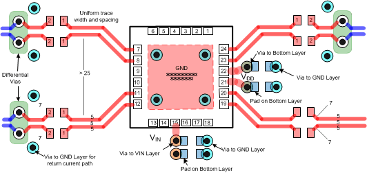 Figure 40. DS100BR111 Example Layout