SNLS338F January 2011 – November 2014 DS100BR111
PRODUCTION DATA.
- 1 Features
- 2 Applications
- 3 Description
- 4 Simplified Schematic
- 5 Revision History
- 6 Pin Configuration and Functions
- 7 Specifications
- 8 Detailed Description
- 9 Application and Implementation
- 10Power Supply Recommendations
- 11Layout
- 12Device and Documentation Support
- 13Mechanical, Packaging, and Orderable Information
パッケージ・オプション
メカニカル・データ(パッケージ|ピン)
- RTW|24
サーマルパッド・メカニカル・データ
- RTW|24
発注情報
6 Pin Configuration and Functions
24-Pin
RTW Package
Top View
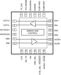
1. The center DAP on the package bottom is the device GND connection. This pad must be connected to GND through multiple (minimum of 4) vias to ensure optimal electrical and thermal performance.
Pin Functions(1)
| PIN | I/O, TYPE | DESCRIPTION | ||
|---|---|---|---|---|
| NAME | NUMBER | |||
| DIFFERENTIAL HIGH SPEED I/O's | ||||
| INA+, INA- , INB+, INB- |
24, 23 11, 12 |
I, CML | Inverting and non-inverting CML differential inputs to the equalizer. On-chip 50 Ω termination resistors connect both INx+ and INx- to VDD. Compatible with AC coupled CML inputs. | |
| OUTA+, OUTA-, OUTB+, OUTB- |
7, 8 20, 19 |
O, CML | Inverting and non-inverting 50 Ω driver outputs with de-emphasis. Compatible with AC coupled CML inputs. | |
| CONTROL PINS | ||||
| ENSMB | 3 | I, 4-LEVEL, LVCMOS |
System Management Bus (SMBus) Enable Pin High = Register Access SMBus Slave Mode Float = Read External EEPROM (SMBus Master Mode) Tie 1 kΩ to GND = Pin Mode |
|
| ENSMB = Float or 1 (SMBus MODES) | ||||
| SCL | 5 | I, 2-LEVEL, LVCMOS, O, Open Drain |
Clock output when loading EEPROM configuration, reverting to SMBus clock input when EEPROM load is complete (ALL_DONE = 0). External 2 kΩ to 5 kΩ pull-up resistor to VDD (2.5 V mode) or VIN (3.3 V mode) recommended as per SMBus interface standards(2) |
|
| SDA | 4 | I, 2-LEVEL, LVCMOS, O, Open Drain |
In both SMBus Modes, this pin is the SMBus data I/O. Data input or open drain output. External 2 kΩ to 5 kΩ pull-up resistor to VDD (2.5 V mode) or VIN (3.3 V mode) recommended as per SMBus interface standards(2) |
|
| AD0-AD3 | 10, 9, 2, 1 | I, 4-LEVEL, LVCMOS |
ENSMB Master or Slave mode SMBus Slave Address Inputs. In SMBus mode, these pins are the user set SMBus slave address inputs. There are 16 addresses supported by these pins. Pins must be tied Low or High when used to define the device SMBus address. (4) |
|
| READEN | 17 | I, 2-LEVEL, LVCMOS |
ENSMB = Float: When using SMBus Master Mode, a logic low on this pin starts the load from the external EEPROM. ENSMB = 1: When using SMBus Slave Mode, the VOD_SEL/READEN pin must be tied Low for the AD[3:0] to be active. If this pin is tied High or left floating, an address of 0xB0 will be used for the DS100BR111. |
|
| DONE | 18 | O, 2-LEVEL, LVCMOS |
When using an External EEPROM (ENSMB = Float), Valid Register Load Status Output High = External EEPROM load failed or incomplete Low = External EEPROM load passed |
|
| ENSMB = 0 (PIN MODE) | ||||
| EQA0, EQA1 EQB0, EQB1 |
10, 9 1, 2 |
I, 4-LEVEL, LVCMOS |
EQA[1:0] and EQB[1:0] control the level of equalization on the input pins. EQA[1:0] controls the A channel, and EQB[1:0] controls the B channel. The pins are only active when ENSMB = 0. When ENSMB = 1, the SMBus registers provide independent control of each channel, and the EQB0/B1 pins are converted to SMBus AD2/AD3 inputs. See Table 3 for additional information. |
|
| DEMA, DEMB | 4, 5 | I, 4-LEVEL, LVCMOS |
DEMA and DEMB control the level of de-emphasis for the output driver when in 10G mode. DEMA controls the A channel, and DEMB controls the B channel. The pins are only active when ENSMB = 0. When ENSMB = 1, the SMBus registers provide independent control of each channel, and the DEM pins are converted to SMBus SCL and SDA pins. See Table 4 for additional information. |
|
| VOD_SEL | 17 | I, 4-LEVEL, LVCMOS |
VOD Select High = 10G-KR Mode (VOD = 1.1 Vpp or 1.3 Vpp) Float = (VOD = 1.0 Vpp) 20 kΩ to GND = (VOD = 1.2 Vpp) 1 kΩ to GND = (VOD = 700 mVpp) See (4)(5) for additional notes. See Table 2 for additional information. |
|
| MODE | 18 | I, 4-LEVEL, LVCMOS |
Controls Device Mode of Operation High= 10GbE Mode, Continuous Talk (Output Always On) Float = 10G-KR Mode, Slow OOB 20 kΩ to GND = eSATA Mode, Fast OOB, Auto Low Power on 100 µs of inactivity. SD stays active. 1 kΩ to GND = SAS Mode, Fast OOB |
|
| CONTROL PINS — BOTH PIN AND SMBus MODES (LVCMOS) | ||||
| TX_DIS | 6 | I, 2-LEVEL, LVCMOS |
High = OUTA Enabled, OUTB Disabled Low = OUTA and OUTB Enabled |
|
| LOS | 13 | O, Open Drain | Indicates Loss of Signal (Default is LOS on INA). Can be modified via SMBus registers. | |
| SD_TH | 14 | I, 4-LEVEL, LVCMOS |
The SD_TH pin controls LOS threshold setting Assert (mVpp), Deassert (mVpp) High = 190 mVpp, 130 mVpp Float = 180 mVpp, 110 mVpp (Default) 20 kΩ to GND = 160 mVpp, 100 mVpp 1 kΩ to GND = 210 mVpp, 150 mVpp(3) |
|
| VDD_SEL | 16 | I, FLOAT | Enables the 3.3 V to 2.5 V internal regulator Low = 3.3 V Operation Float = 2.5 V Operation |
|
| POWER | ||||
| VDD | 21, 22 | Power | Power supply pins When in 2.5 V mode, connect to 2.5 V supply. When in 3.3 V mode, do not connect to any supply voltage. Should be used to attach external decoupling to device, 100 nF recommended. See Power Supply Recommendations for additional information. |
|
| VIN | 15 | Power | VIN = 3.3 V ± 10% (input to internal LDO regulator) When in 2.5 V mode, VIN pin must be left floating. See Power Supply Recommendations for additional information. |
|
| GND | DAP | Power | Ground pad (DAP - die attach pad). | |
(1) LVCMOS inputs without the “Float” conditions must be driven to a logic low or high at all times or operation is not ensured. Unless the "Float" level is desired, 4-Level input pins require a minimum 1 kΩ resistor to GND, VDD (in 2.5 V mode), or VIN (in 3.3 V mode). Input edge rate for LVCMOS/FLOAT inputs must be faster than 50 ns from 10–90%.
(2) SCL and SDA pins can be tied either to 3.3 V or 2.5 V, regardless of whether the device is operating in 2.5 V mode or 3.3 V mode.
(3) Using values less than the default level can extend the time required to detect LOS and are not recommended.
(4) Setting VOD_SEL = High in SMBus Mode will force the SMBus Address = 0xB0
(5) DS100BR111 OUTA is limited to 700 mVpp in pin mode.