SNLS399B January 2012 – January 2015 DS100DF410
PRODUCTION DATA.
- 1 Features
- 2 Applications
- 3 Description
- 4 Revision History
- 5 Pin Configuration and Functions
- 6 Specifications
-
7 Detailed Description
- 7.1 Overview
- 7.2 Functional Block Diagram
- 7.3
Feature Description
- 7.3.1 Device Data Path Operation
- 7.3.2 Signal Detect
- 7.3.3 CTLE
- 7.3.4 DFE
- 7.3.5 Clock and Data Recovery
- 7.3.6 Output Driver
- 7.3.7 CTLE Boost Setting
- 7.3.8 DFE Tap Weight and Polarity Setting
- 7.3.9 Driver Output Voltage
- 7.3.10 Driver Output De-Emphasis
- 7.3.11 Driver Output Rise/Fall Time
- 7.3.12 Ref_mode 0 Mode (Reference Clock Not Required)
- 7.3.13 Ref_mode 3 Mode (Reference Clock Required)
- 7.3.14 False Lock Detector Setting
- 7.3.15 Reference Clock In
- 7.3.16 Reference Clock Out
- 7.3.17 Daisy Chain of REFCLK_OUT to REFCLK_IN
- 7.3.18 INT
- 7.3.19 LOCK_3, LOCK_2, LOCK_1, and LOCK_0
- 7.4 Device Functional Modes
- 7.5
Programming
- 7.5.1 SMBus Strap Observation
- 7.5.2 Device Revision and Device ID
- 7.5.3 Control/Shared Register Reset
- 7.5.4 Interrupt Channel Flag Bits
- 7.5.5 SMBus Master Mode Control Bits
- 7.5.6 Resetting Individual Channels of the Retimer
- 7.5.7 Interrupt Status
- 7.5.8 Overriding the CTLE Boost Setting
- 7.5.9 Overriding the VCO CAP DAC Values
- 7.5.10 Overriding the Output Multiplexer
- 7.5.11 Overriding the VCO Divider Selection
- 7.5.12 Using the PRBS Generator
- 7.5.13 Using the Internal Eye Opening Monitor
- 7.5.14 Overriding the DFE Tap Weights and Polarities
- 7.5.15 Enabling Slow Rise/Fall Time on the Output Driver
- 7.5.16 Inverting the Output Polarity
- 7.5.17 Overriding the Figure of Merit for Adaptation
- 7.5.18 Setting the Rate and Subrate for Lock Acquisition
- 7.5.19 Setting the Adaptation/Lock Mode
- 7.5.20 Initiating Adaptation
- 7.5.21 Setting the Reference Enable Mode
- 7.5.22 Overriding the CTLE Settings Used for CTLE Adaptation
- 7.5.23 Setting the Output Differential Voltage
- 7.5.24 Setting the Output De-emphasis Setting
- 7.6 Register Maps
- 8 Application and Implementation
- 9 Power Supply Recommendations
- 10Layout
- 11Device and Documentation Support
- 12Mechanical, Packaging, and Orderable Information
1 Features
- Each Channel Independently Locks to 10.3125 Gbps
- Lock Operation (typically under 15 ms)
- Low Latency (~300 ps)
- Adaptive Equalization up to 34 dB Boost at 5 GHz
- Adjustable Transmit VOD: 600 to 1300 mVp-p
- Adjustable Transmit De-emphasis to –12 dB
- Typical Power Dissipation (EQ+DFE+CDR+DE): 180 mW/channel
- Programmable Output Polarity Inversion
- Input Signal Detection, CDR Lock Detection/Indicator
- On-chip Eye Monitor (EOM), PRBS Generator
- Single 2.5 V ±5% Power Supply
- SMBus/EEPROM Configuration Modes
- Operating Temperature Range of –40°C to 85°C
- WQFN 48-Pin, 7 mm x 7 mm Package
- Easy Pin Compatible Upgrade Between Repeater and Retimers
- DS100RT410 (EQ+CDR+DE): 10.3125 Gbps
- DS100DF410 (EQ+DFE+CDR+DE): 10.3125 Gbps
- DS110RT410 (EQ+CDR+DE): 8.5–11.3 Gbps
- DS110DF410 (EQ+DFE+CDR+DE): 8.5–11.3 Gbps
- DS125RT410 (EQ+CDR+DE): 9.8–12.5 Gbps
- DS125DF410 (EQ+DFE+CDR+DE): 9.8–12.5 Gbps
- DS100BR410 (EQ+DE): Up to 10.3125 Gbps
2 Applications
- Front Port SFF 8431 (SFP+) Optical and Direct Attach Copper
- Backplane Reach Extension, Data Retimer
- Ethernet: 10GbE, 1GbE
For other data rates and data transmission protocols, other pin-compatible devices in the retimer family can be used.
3 Description
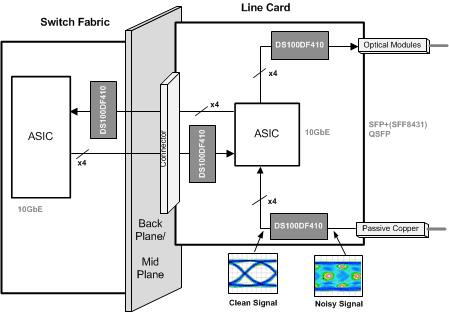
The DS100DF410 is four channel retimers with integrated signal conditioning. Each channel can independently lock to 10.3125 Gbps data rate to support 10GbE. The device includes a fully adaptive Continuous-Time Linear Equalizer (CTLE), Clock and Data Recovery (CDR) and transmit De-Emphasis (DE) driver. The DS100DF410 also includes a self calibrating 5-tap Decision Feedback Equalizer (DFE) to enable data transmission over long, lossy and crosstalk-impaired highspeed serial links to achieve BER < 1×10-15.
The programmable settings can be applied easily using the SMBus (I2C) interface, or they can be loaded via an external EEPROM. An on-chip eye monitor and a PRBS generator allow real-time measurement of high-speed serial data for system bring-up or field tuning. Flow-through pinout and single power supply make the DS100DF410 easy to use.
Device Information(1)
| PART NUMBER | PACKAGE | BODY SIZE (NOM) |
|---|---|---|
| DS100DF410SQ | WQFN (48) | 7.00 mm × 7.00 mm |
- For all available packages, see the orderable addendum at the end of the data sheet.
Typical Application Diagram
4 Revision History
Changes from A Revision (February 2013) to B Revision
- Changed ESD Ratings table, Feature Description section, Device Functional Modes, Application and Implementation section, Power Supply Recommendations section, Layout section, Device and Documentation Support section, and Mechanical, Packaging, and Orderable Information sectionGo