SNLS231O September 2006 – April 2015 DS90UR124-Q1 , DS90UR241-Q1
PRODUCTION DATA.
- 1 Features
- 2 Applications
- 3 Description
- 4 Revision History
- 5 Description (continued)
- 6 Pin Configuration and Functions
- 7 Specifications
-
8 Detailed Description
- 8.1 Overview
- 8.2 Functional Block Diagram
- 8.3 Feature Description
- 8.4 Device Functional Modes
- 9 Application and Implementation
- 10Power Supply Recommendations
- 11Layout
- 12Device and Documentation Support
- 13Mechanical, Packaging, and Orderable Information
6 Pin Configuration and Functions
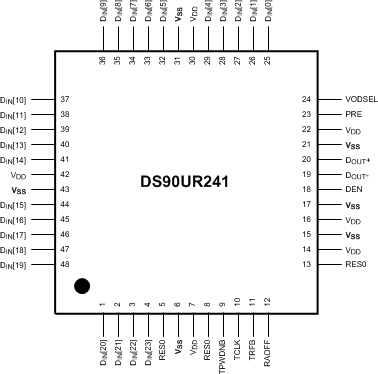
PFB Package
48-Pin TQFP
Top View
 Figure 1. DS90UR241 Serializer
Pin Functions: PFB Package
| PIN | I/O | DESCRIPTION | |
|---|---|---|---|
| NO. | NAME | ||
| LVCMOS PARALLEL INTERFACE PINS | |||
| 4-1, 48-44, 41-32, 29-25 | DIN[23:0] | LVCMOS_I | Transmitter Parallel Interface Data Input Pins. Tie LOW if unused; do not float. |
| 10 | TCLK | LVCMOS_I | Transmitter Parallel Interface Clock Input Pin. Strobe edge set by TRFB configuration pin. |
| CONTROL AND CONFIGURATION PINS | |||
| 18 | DEN | LVCMOS_I | Transmitter Data Enable DEN = H; LVDS Driver Outputs are Enabled (ON). DEN = L; LVDS Driver Outputs are Disabled (OFF), Transmitter LVDS Driver DOUT (+/-) Outputs are in Tri-state, PLL still operational and locked to TCLK. |
| 23 | PRE | LVCMOS_I | Pre-emphasis Level Select PRE = NC (No Connect); Pre-emphasis is Disabled (OFF). Pre-emphasis is active when input is tied to VSS through external resistor RPRE. Resistor value determines pre-emphasis level. Recommended value RPRE ≥ 6 kΩ; Imax = [48 / RPRE], RPREmin = 6 kΩ |
| 12 | RAOFF | LVCMOS_I | Randomizer Control Input Pin RAOFF = H, Backwards compatible mode for use with DS90C124 Deserializer. RAOFF = L; Additional randomization ON (Default), Selects 2E7 LSFR setting. See Table 1 for more details. |
| 5, 8, 13 | RES0 | LVCMOS_I | Reserved. This pin must be tied LOW. |
| 9 | TPWDNB | LVCMOS_I | Transmitter Power Down Bar TPWDNB = H; Transmitter is Enabled and ON TPWDNB = L; Transmitter is in power down mode (Sleep), LVDS Driver DOUT (+/-) Outputs are in Tri-state stand-by mode, PLL is shutdown to minimize power consumption. |
| 11 | TRFB | LVCMOS_I | Transmitter Clock Edge Select Pin TRFB = H; Parallel Interface Data is strobed on the Rising Clock Edge. TRFB = L; Parallel Interface Data is strobed on the Falling Clock Edge |
| 24 | VODSEL | LVCMOS_I | VOD Level Select VODSEL = L; LVDS Driver Output is ±500 mV (RL = 100 Ω) VODSEL = H; LVDS Driver Output is ±900 mV (RL = 100 Ω) For normal applications, set this pin LOW. For long cable applications where a larger VOD is required, set this pin HIGH. |
| LVDS SERIAL INTERFACE PINS | |||
| 20 | DOUT+ | LVDS_O | Transmitter LVDS True (+) Output. This output is intended to be loaded with a 100-Ω load to the DOUT+ pin. The interconnect should be AC coupled to this pin with a 100-nF capacitor. |
| 19 | DOUT− | LVDS_O | Transmitter LVDS Inverted (-) Output This output is intended to be loaded with a 100-Ω load to the DOUT- pin. The interconnect should be AC coupled to this pin with a 100-nF capacitor. |
| POWER / GROUND PINS | |||
| 22 | VDD | VDD | Analog Voltage Supply, LVDS Output POWER |
| 16 | VDD | VDD | Analog Voltage Supply, VCO POWER |
| 14 | VDD | VDD | Analog Voltage Supply, PLL POWER |
| 30 | VDD | VDD | Digital Voltage Supply, Serializer POWER |
| 7 | VDD | VDD | Digital Voltage Supply, Serializer Logic POWER |
| 42 | VDD | VDD | Digital Voltage Supply, Serializer INPUT POWER |
| 21 | VSS | GND | Analog Ground, LVDS Output GROUND |
| 17 | VSS | GND | Analog Ground, VCO GROUND |
| 15 | VSS | GND | Analog Ground, PLL GROUND |
| 31 | VSS | GND | Digital Ground, Serializer GROUND |
| 6 | VSS | GND | Digital Ground, Serializer Logic GROUND |
| 43 | VSS | GND | Digital Ground, Serializer Input GROUND |
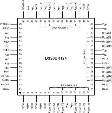
PAG Package
64-Pin TQFP
Top View
 Figure 2. DS90UR124 Deserializer
Pin Functions: PAG Package
| PIN | I/O | DESCRIPTION | |
|---|---|---|---|
| NO. | NAME | ||
| LVCMOS PARALLEL INTERFACE PINS | |||
| 24 | RCLK | LVCMOS_O | Parallel Interface Clock Output Pin. Strobe edge set by RRFB configuration pin. |
| 35-38, 41-44 | ROUT[7:0] | LVCMOS_O | Receiver Parallel Interface Data Outputs – Group 1 |
| 19-22, 27-30 | ROUT[15:8] | LVCMOS_O | Receiver Parallel Interface Data Outputs – Group 2 |
| 7-10, 13-16 | ROUT[23:16] | LVCMOS_O | Receiver Parallel Interface Data Outputs – Group 3 |
| CONTROL AND CONFIGURATION PINS | |||
| 23 | LOCK | LVCMOS_O | LOCK indicates the status of the receiver PLL LOCK = H; receiver PLL is locked LOCK = L; receiver PLL is unlocked, ROUT[23-0] and RCLK are at Tri-state. |
| 49 | PTOSEL | LVCMOS_I | Progressive Turn On Operation Selection PTO = H; ROUT[23:0] are grouped into three groups of eight, with each group switching about ±1 UI to ±2 UI apart relative to RCLK. (Figure 17) PTO = L; PTO Spread Mode, ROUT[23:0] outputs are spread ±1 UI to ±2 UI and RCLK spread ±1 UI. (Figure 18) See Applications Informations section for more details. |
| 63 | RAOFF | LVCMOS_I | Randomizer Control Input Pin (See Table 2 for more details.) RAOFF = H, Backwards compatible mode for use with DS90C241 Serializer. RAOFF = L; Additional randomization ON (Default), Selects 2E7 LSFR setting. |
| 60 | REN | LVCMOS_I | Receiver Data Enable REN = H; ROUT[23-0] and RCLK are Enabled (ON). REN = L; ROUT[23-0] and RCLK are Disabled (OFF), Receiver ROUT[23-0] and RCLK Outputs are in Tri-state, PLL still operational and locked to TCLK. |
| 50 | RES0 | LVCMOS_I | Reserved. This pin MUST be tied LOW. |
| 1-6, 17, 18, 33, 34 | RES0 | NC | No Connection. Pins are not physically connected to the die. Recommendation is to leave pin open or tie it to LOW. |
| 48 | RPWDNB | LVCMOS_I | Receiver Power Down Bar RPWDNB = H; Receiver is Enabled and ON RPWDNB = L; Receiver is in power down mode (Sleep), ROUT[23-0], RCLK, and LOCK are in Tri-state standby mode, PLL is shutdown to minimize power consumption. |
| 55 | RRFB | LVCMOS_I | Receiver Clock Edge Select Pin RRFB = H; ROUT LVCMOS Outputs strobed on the Rising Clock Edge. RRFB = L; ROUT LVCMOS Outputs strobed on the Falling Clock Edge. |
| 64 | SLEW | LVCMOS_I | LVCMOS Output Slew Rate Control SLEW = L; Low drive output at 2 mA (default) SLEW = H; High drive output at 4 mA |
| BIST MODE PINS (See Application and Implementation for more details.) | |||
| 61 | BISTEN | LVCMOS_I | Control Pin for BIST Mode Enable BISTEN = L; Default at Low, Normal Mode. BISTEN = H; BIST mode active. When BISTEN = H and DS90UR241 DIN[23:0] = Low or Floating; device will go to BIST mode accordingly. Check PASS output pin for test status. |
| 62 | BISTM | LVCMOS_I | BIST Mode selection. Control pin for which Deserializer is set for BIST reporting mode. BISTM = L; Default at Low, Status of all ROUT with respective bit error on cycle-by-cycle basis BISTM = H; Total accumulated bit error count provided on ROUT[7:0] (binary counter up to 255) |
| 45 | PASS | LVCMOS_O | Pass flag output for @Speed BIST Test operation. PASS = L; BIST failure PASS = H; LOCK = H before BIST can be enabled, then 1x10⁻⁹ error rate achieved across link. |
| LVDS SERIAL INTERFACE PINS | |||
| 53 | RIN+ | LVDS_I | Receiver LVDS True (+) Input — This input is intended to be terminated with a 100Ω load to the RIN+ pin. The interconnect should be AC Coupled to this pin with a 100 nF capacitor. |
| 54 | RIN− | LVDS_I | Receiver LVDS Inverted (−) Input — This input is intended to be terminated with a 100Ω load to the RIN- pin. The interconnect should be AC Coupled to this pin with a 100 nF capacitor. |
| POWER / GROUND PINS | |||
| 51 | VDD | VDD | Analog LVDS Voltage Supply, POWER |
| 59 | VDD | VDD | Analog Voltage Supply, PLL POWER |
| 57 | VDD | VDD | Analog Voltage supply, PLL VCO POWER |
| 32 | VDD | VDD | Digital Voltage Supply, LOGIC POWER |
| 46 | VDD | VDD | Digital Voltage Supply, LOGIC POWER |
| 40 | VDD | VDD | Digital Voltage Supply, LVCMOS Output POWER |
| 26 | VDD | VDD | Digital Voltage Supply, LVCMOS Output POWER |
| 11 | VDD | VDD | Digital Voltage Supply, LVCMOS Output POWER |
| 52 | VSS | GND | Analog LVDS GROUND |
| 58 | VSS | GND | Analog Ground, PLL GROUND |
| 56 | VSS | GND | Analog Ground, PLL VCO GROUND |
| 31 | VSS | GND | Digital Ground, Logic GROUND |
| 47 | VSS | GND | Digital Ground, LOGIC GROUND |
| 39 | VSS | GND | Digital Ground, LVCMOS Output GROUND |
| 25 | VSS | GND | Digital Ground, LVCMOS Output GROUND |
| 12 | VSS | GND | Digital Ground, LVCMOS Output GROUND |