SNLS231O September 2006 – April 2015 DS90UR124-Q1 , DS90UR241-Q1
PRODUCTION DATA.
- 1 Features
- 2 Applications
- 3 Description
- 4 Revision History
- 5 Description (continued)
- 6 Pin Configuration and Functions
- 7 Specifications
-
8 Detailed Description
- 8.1 Overview
- 8.2 Functional Block Diagram
- 8.3 Feature Description
- 8.4 Device Functional Modes
- 9 Application and Implementation
- 10Power Supply Recommendations
- 11Layout
- 12Device and Documentation Support
- 13Mechanical, Packaging, and Orderable Information
7 Specifications
7.1 Absolute Maximum Ratings
over operating free-air temperature range (unless otherwise noted) (1)| MIN | MAX | UNIT | |||||
|---|---|---|---|---|---|---|---|
| Supply Voltage (VDD) | –0.3 | 4 | V | ||||
| LVCMOS Input Voltage | –0.3 | VDD +0.3 | V | ||||
| LVCMOS Output Voltage | –0.3 | VDD +0.3 | V | ||||
| LVDS Receiver Input Voltage | –0.3 | +3.9 | V | ||||
| LVDS Driver Output Voltage | –0.3 | +3.9 | V | ||||
| LVDS Output Short Circuit Duration | 10 | ms | |||||
| Junction Temperature | 150 | °C | |||||
| Lead Temperature (Soldering, 4 seconds) | 260 | °C | |||||
| Maximum Package Power Dissipation Capacity(2) | Package Derating: |
DS90UR241 − 48L TQFP | RθJA | 45.8 (4L); 75.4 (2L) |
°C/W | ||
| RθJC | 21.0 | ||||||
| DS90UR124 − 64L TQFP | RθJA | 42.8 (4L); 67.2 (2L) |
|||||
| RθJC | 14.6 | ||||||
| Storage temperature, Tstg | –65 | 150 | °C | ||||
(1) Stresses beyond those listed under Absolute Maximum Ratings may cause permanent damage to the device. These are stress ratings only, which do not imply functional operation of the device at these or any other conditions beyond those indicated under Recommended Operating Conditions. Exposure to absolute-maximum-rated conditions for extended periods may affect device reliability.
(2) 1/RθJA °C/W above +25°C
7.2 ESD Ratings
| VALUE | UNIT | |||||
|---|---|---|---|---|---|---|
| DS90UR241-Q1 IN PFB PACKAGE | ||||||
| V(ESD) | Electrostatic discharge | Human body model (HBM), per AEC Q100-002(1) | All pins | ≥±8000 | V | |
| Charged device model (CDM), per AEC Q100-011 | Corner pins (1, 12, 13, 24, 25, 36, 37, and 48) | ±12500 | ||||
| Other pins | ±12500 | |||||
| (ISO10605)(2) | Contact Discharge (20, 19) | ±10000 | ||||
| Air Discharge (20, 19) | ±30000 | |||||
| DS90UR124-Q1 IN PAG PACKAGE | ||||||
| V(ESD) | Electrostatic discharge | Human body model (HBM), per AEC Q100-002(1) | All pins | ≥±8000 | V | |
| Charged device model (CDM), per AEC Q100-011 | Corner pins (1, 16, 17, 32, 33, 48, 49, and 64) | ±12500 | ||||
| Other pins | ±12500 | |||||
| (ISO10605)(2) | Contact Discharge (RIN+, RIN−) | ±10000 | ||||
| Air Discharge (RIN+, RIN−) | ±30000 | |||||
(1) AEC Q100-002 indicates HBM stressing is done in accordance with the ANSI/ESDA/JEDEC JS-001 specification.
(2) RD = 2 kΩ, CS = 330 pF
7.3 Recommended Operating Conditions
over operating free-air temperature range (unless otherwise noted)| MIN | NOM | MAX | UNIT | |
|---|---|---|---|---|
| Supply Voltage (VDD) | 3.0 | 3.3 | 3.6 | V |
| Operating Free Air Temperature (TA) | –40 | 25 | 105 | °C |
| Clock Rate | 5 | 43 | MHz | |
| Supply Noise | ±100 | mVP-P |
7.4 Thermal Information
| THERMAL METRIC(1) | DS90UR124-Q1 | DS90UR241-Q1 | UNIT | |
|---|---|---|---|---|
| PAG [TQFP] | PFB [TQFP] | |||
| 64 PINS | 48 PINS | |||
| RθJA | Junction-to-ambient thermal resistance | 58.1 | 64.3 | °C/W |
| RθJC(top) | Junction-to-case (top) thermal resistance | 13.0 | 14.1 | |
| RθJB | Junction-to-board thermal resistance | 30.4 | 30.2 | |
| ψJT | Junction-to-top characterization parameter | 0.3 | 0.4 | |
| ψJB | Junction-to-board characterization parameter | 30.0 | 29.8 | |
(1) For more information about traditional and new thermal metrics, see the IC Package Thermal Metrics application report, SPRA953.
7.5 Electrical Characteristics
over recommended operating supply and temperature ranges unless otherwise specified| PARAMETER | TEST CONDITIONS | PIN/FREQ. | MIN | TYP | MAX | UNIT | ||
|---|---|---|---|---|---|---|---|---|
| LVCMOS DC SPECIFICATIONS | ||||||||
| VIH | High-Level Input Voltage | Tx: DIN[0:23], TCLK, TPWDNB, DEN, TRFB, RAOFF, VODSEL, RES0. Rx: RPWDNB, RRFB, REN, PTOSEL, BISTEN, BISTM, SLEW, RES0. |
2 | VDD | V | |||
| VIL | Low-Level Input Voltage | GND | 0.8 | V | ||||
| VCL | Input Clamp Voltage | ICL = −18 mA | –0.8 | –1.5 | V | |||
| IIN | Input Current | VIN = 0 V or 3.6 V | Tx: DIN[0:23], TCLK, TPWDNB, DEN, TRFB, RAOFF, RES0. Rx: RRFB, REN, PTOSEL, BISTEN, BISTM, SLEW, RES0. |
–10 | ±2 | 10 | µA | |
| Rx: RPWDNB | –20 | ±5 | 20 | |||||
| VOH | High-Level Output Voltage | IOH = −2 mA, SLEW = L IOH = −4 mA, SLEW = H |
Rx: ROUT[0:23], RCLK, LOCK, PASS. | 2.3 | 3 | VDD | V | |
| VOL | Low-Level Output Voltage | IOL = 2 mA, SLEW = L IOL = 4 mA, SLEW = H |
GND | 0.33 | 0.5 | V | ||
| IOS | Output Short Circuit Current | VOUT = 0 V | –40 | –70 | –110 | mA | ||
| IOZ | Tri-state Output Current | RPWDNB, REN = 0 V, VOUT = 0 V or VDD |
Rx: ROUT[0:23], RCLK, LOCK, PASS. | –30 | ±0.4 | 30 | µA | |
| LVDS DC SPECIFICATIONS | ||||||||
| VTH | Differential Threshold High Voltage | VCM = 1.8 V | Rx: RIN+, RIN− | 50 | mV | |||
| VTL | Differential Threshold Low Voltage | –50 | mV | |||||
| IIN | Input Current | VIN = 2.4 V, VDD = 3.6 V | ±100 | ±250 | µA | |||
| VIN = 0 V, VDD = 3.6 V | ±100 | ±250 | ||||||
| VOD | Output Differential Voltage (DOUT+)–(DOUT−) | RL = 100 Ω, without pre-emphasis Figure 12 | VODSEL = L | Tx: DOUT+, DOUT− | 380 | 500 | 630 | mV |
| VODSEL = H | 500 | 900 | 1100 | |||||
| ΔVOD | Output Differential Voltage Unbalance | RL = 100 Ω, without pre-emphasis |
VODSEL = L | 1 | 50 | mV | ||
| VODSEL = H | ||||||||
| VOS | Offset Voltage | RL = 100 Ω, without pre-emphasis |
VODSEL = L | 1 | 1.25 | 1.50 | V | |
| VODSEL = H | ||||||||
| ΔVOS | Offset Voltage Unbalance | RL = 100 Ω, without pre-emphasis |
VODSEL = L | 3 | 50 | mV | ||
| VODSEL = H | ||||||||
| IOS | Output Short Circuit Current | DOUT = 0 V, DIN = H, TPWDNB = 2.4 V |
VODSEL = L | –2 | –5 | –8 | mA | |
| VODSEL = H | –4.5 | –7.9 | –14 | |||||
| IOZ | Tri-state Output Current | TPWDNB = 0 V, DOUT = 0 V OR VDD |
–15 | ±1 | 15 | µA | ||
| TPWDNB = 2.4 V, DEN = 0 V DOUT = 0 V OR VDD |
–15 | ±1 | 15 | |||||
| TPWDNB = 2.4 V, DEN = 2.4 V, DOUT = 0 V OR VDD NO LOCK (NO TCLK) |
–15 | ±1 | 15 | |||||
| SER/DES SUPPLY CURRENT (DVDD*, PVDD* AND AVDD* PINS) *DIGITAL, PLL, AND ANALOG VDDS | ||||||||
| IDDT | Serializer Total Supply Current (includes load current) |
RL = 100 Ω, PRE = OFF, RAOFF = H, VODSEL = L |
f = 43 MHz, checkerboard pattern Figure 3 |
60 | 85 | mA | ||
| RL = 100 Ω, PRE = 12 kΩ, RAOFF = H, VODSEL = L |
65 | 90 | ||||||
| RL = 100 Ω, PRE = OFF, RAOFF = H, VODSEL = H |
f = 43 MHz, random pattern |
66 | 90 | |||||
| IDDTZ | Serializer Supply Current Power-down |
TPWDNB = 0V (All other LVCMOS Inputs = 0 V) |
45 | µA | ||||
| IDDR | Deserializer Total Supply Current (includes load current) |
CL = 4 pF, SLEW = H |
f = 43 MHz, checkerboard pattern LVCMOS Output Figure 4 |
85 | 105 | mA | ||
| CL = 4 pF, SLEW = H |
f = 43 MHz, random pattern LVCMOS Output |
80 | 100 | |||||
| IDDRZ | Deserializer Supply Current Power-down |
RPWDNB = 0 V (All other LVCMOS Inputs = 0 V, RIN+/RIN- = 0 V) |
50 | µA | ||||
7.6 Serializer Input Timing Requirements for TCLK
over recommended operating supply and temperature ranges unless otherwise specified| MIN | NOM | MAX | UNIT | |||
|---|---|---|---|---|---|---|
| tTCP | Transmit Clock Period | Figure 7 | 23.25 | T | 200 | ns |
| tTCIH | Transmit Clock High Time | 0.3 T | 0.5 T | 0.7 T | ns | |
| tTCIL | Transmit Clock Low Time | 0.3 T | 0.5 T | 0.7 T | ns | |
| tCLKT | TCLK Input Transition Time | Figure 6 | 2.5 | ns | ||
| tJIT | TCLK Input Jitter | f = 43 MHz | ±100 | ps | ||
| f = 33 MHz | ±130 | |||||
7.7 Serializer Switching Characteristics
over recommended operating supply and temperature ranges unless otherwise specified| PARAMETER | TEST CONDITIONS | MIN | TYP | MAX | UNIT | |
|---|---|---|---|---|---|---|
| tLLHT | LVDS Low-to-High Transition Time | RL = 100 Ω, VODSEL = L, CL = 10 pF to GND, Figure 5 |
245 | 550 | ps | |
| tLHLT | LVDS High-to-Low Transition Time | 264 | 550 | ps | ||
| tDIS | DIN (0:23) Setup to TCLK | RL = 100 Ω, CL = 10 pF to GND Figure 7 |
4 | ns | ||
| tDIH | DIN (0:23) Hold from TCLK | 4 | ns | |||
| tHZD | DOUT ± HIGH to Tri-state Delay | RL = 100 Ω, CL = 10 pF to GND Figure 8 |
10 | 15 | ns | |
| tLZD | DOUT ± LOW to Tri-state Delay | 10 | 15 | ns | ||
| tZHD | DOUT ± Tri-state to HIGH Delay | 75 | 150 | ns | ||
| tZLD | DOUT ± Tri-state to LOW Delay | 75 | 150 | ns | ||
| tPLD | Serializer PLL Lock Time | RL = 100 Ω | 10 | ms | ||
| tSD | Serializer Delay | RL = 100 Ω, PRE = OFF, RAOFF = L, TRFB = H, Figure 10 |
3.5T+2 | 3.5T+10 | ns | |
| RL = 100 Ω, PRE = OFF, RAOFF = L, TRFB = L, Figure 10 |
3.5T+2 | 3.5T+10 | ||||
| TxOUT_E_O | TxOUT_Eye_Opening. TxOUT_E_O centered on (tBIT/)2 |
5 MHz–43 MHz, RL = 100 Ω, CL = 10 pF to GND, RANDOM pattern Figure 11 |
0.76 | 0.84 | UI | |
7.8 Deserializer Switching Characteristics
over recommended operating supply and temperature ranges unless otherwise specified| PARAMETER | TEST CONDITIONS | PIN/FREQ. | MIN | TYP | MAX | UNIT | |
|---|---|---|---|---|---|---|---|
| tRCP | Receiver out Clock Period | tRCP = tTCP, PTOSEL = H |
RCLK Figure 17 |
23.25 | T | 200 | ns |
| tRDC | RCLK Duty Cycle | PTOSEL = H, SLEW = L |
45% | 50% | 55% | ||
| tCLH | LVCMOS Low-to-High Transition Time | CL = 4 pF (lumped load), SLEW = H |
ROUT [0:23], RCLK, LOCK |
1.5 | 2.5 | ns | |
| tCHL | LVCMOS High-to-Low Transition Time | 1.5 | 2.5 | ns | |||
| tCLH | LVCMOS Low-to-High Transition Time | CL = 4 pF (lumped load), SLEW = L |
ROUT [0:23], RCLK, LOCK |
2.0 | 3.5 | ns | |
| tCHL | LVCMOS High-to-Low Transition Time | 2.0 | 3.5 | ns | |||
| tROS | ROUT (0:7) Setup Data to RCLK (Group 1) | PTOSEL = L, SLEW = H, Figure 18 |
ROUT[0:7] | (0.35)× tRCP | (0.5×tRCP)–3 UI | ns | |
| tROH | ROUT (0:7) Hold Data to RCLK (Group 1) | (0.35)× tRCP | (0.5×tRCP)–3 UI | ns | |||
| tROS | ROUT (8:15) Setup Data to RCLK (Group 2) | PTOSEL = L, SLEW = H, Figure 18 |
ROUT [8:15], LOCK | (0.35)× tRCP | (0.5×tRCP)–3 UI | ns | |
| tROH | ROUT (8:15) Hold Data to RCLK (Group 2) | (0.35)× tRCP | (0.5×tRCP)–3 UI | ns | |||
| tROS | ROUT (16:23) Setup Data to RCLK (Group 3) | ROUT [16:23] | (0.35)× tRCP | (0.5×tRCP)–3 UI | ns | ||
| tROH | ROUT (16:23) Setup Data to RCLK (Group 3) | (0.35)× tRCP | (0.5×tRCP)–3 UI | ns | |||
| tROS | ROUT (0:7) Setup Data to RCLK (Group 1) | PTOSEL = H, SLEW = H, Figure 17 |
ROUT[0:7] | (0.35)× tRCP | (0.5×tRCP)–2 UI | ns | |
| tROH | ROUT (0:7) Hold Data to RCLK (Group 1) | (0.35)× tRCP | (0.5×tRCP)+2 UI | ns | |||
| tROS | ROUT (8:15) Setup Data to RCLK (Group 2) | ROUT [8:15], LOCK | (0.35)× tRCP | (0.5×tRCP)−1 UI | ns | ||
| tROH | ROUT (8:15) Hold Data to RCLK (Group 2) | (0.35)× tRCP | (0.5×tRCP)+1 UI | ns | |||
| tROS | ROUT (16:23) Setup Data to RCLK (Group 3) | ROUT [16:23] | (0.35)× tRCP | (0.5×tRCP)+1 UI | ns | ||
| tROH | ROUT (16:23) Setup Data to RCLK (Group 3) | (0.35)× tRCP | (0.5×tRCP)–1 UI | ns | |||
| tHZR | HIGH to Tri-state Delay | PTOSEL = H, Figure 16 |
ROUT [0:23], RCLK, LOCK |
3 | 10 | ns | |
| tLZR | LOW to Tri-state Delay | 3 | 10 | ns | |||
| tZHR | Tri-state to HIGH Delay | 3 | 10 | ns | |||
| tZLR | Tri-state to LOW Delay | 3 | 10 | ns | |||
| tDD | Deserializer Delay | PTOSEL = H, Figure 14 |
RCLK | [5+(5/56)]T+3.7 | [5+(5/56)]T +8 | ns | |
| tDSR | Deserializer PLL Lock Time from Powerdown | See Figure 16 | 5 MHz | 128k*T | ms | ||
| 43 MHz | 128k*T | ||||||
| RxIN_TOL-L | Receiver INput TOLerance Left | See Figure 19 |
5 MHz–43 MHz | 0.25 | UI | ||
| RxIN_TOL-R | Receiver INput TOLerance Right | See Figure 19 |
5 MHz–43 MHz | 0.25 | UI | ||
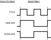 Figure 3. Serializer Input Checkerboard Pattern
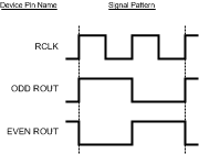 Figure 4. Deserializer Output Checkerboard Pattern
 Figure 5. Serializer LVDS Output Load and Transition Times
 Figure 6. Serializer Input Clock Transition Times
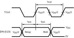 Figure 7. Serializer Setup and Hold Times
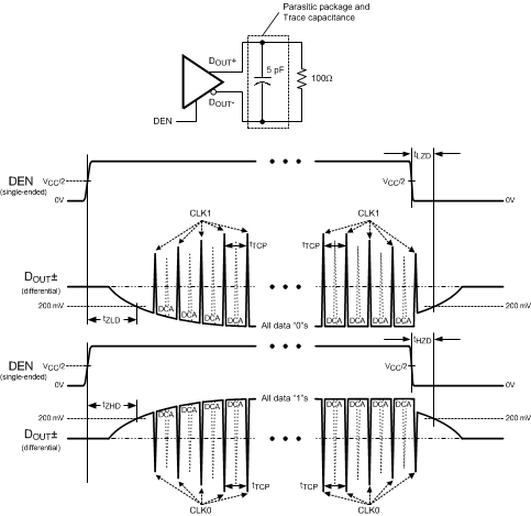 Figure 8. Serializer Tri-State Test Circuit and Delay
 Figure 9. Serializer PLL Lock Time, and TPWDNB Tri-State Delays
 Figure 10. Serializer Delay
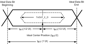 Figure 11. Transmitter Output Eye Opening (TxOUT_E_O)
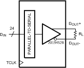
VOD = (DOUT+) – (DOUT−)
Differential output signal is shown as (DOUT+) – (DOUT−), device in Data Transfer mode.
Figure 12. Serializer VOD Diagram
 Figure 13. Deserializer LVCMOS Output Load and Transition Times
 Figure 14. Deserializer Delay
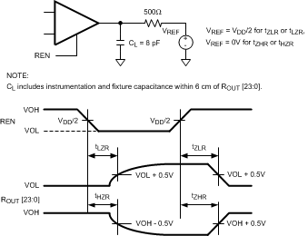 Figure 15. Deserializer Tri-State Test Circuit and Timing
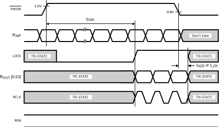 Figure 16. Deserializer PLL Lock Times and RPWDNB Tri-State Delay
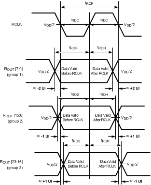 Figure 17. Deserializer Setup and Hold Times and PTO, PTOSEL = H
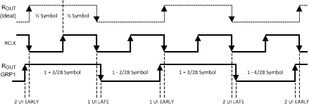
Group 1 will be latched internally by sequence of (early 2UI, late 1UI, early 1UI, late 2UI).
Group 2 will be latched internally by sequence of (late 1UI, early 1UI, late 2UI, early 2UI).
Group 3 will be latched internally by sequence of (early 1UI, late 2UI, early 2UI, late 1UI).
Figure 18. Deserializer Setup and Hold Times and PTO Spread, PTOSEL = L
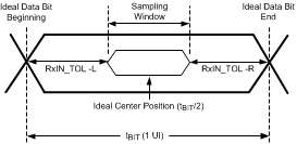
RxIN_TOL_L is the ideal noise margin on the left of the figure, with respect to ideal.
RxIN_TOL_R is the ideal noise margin on the right of the figure, with respect to ideal.
Figure 19. Receiver Input Tolerance (RxIN_TOL) and Sampling Window
7.9 Typical Characteristics
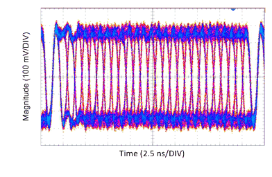 Figure 20. DS90UR241 DOUT± With PCLK at 43 MHz Measured at RIN± Termination
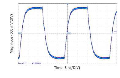 Figure 21. DS90UR124 PCLK Output at 43 MHz