SNLS302E May 2010 – February 2015 DS92LV2411 , DS92LV2412
PRODUCTION DATA.
- 1 Features
- 2 Applications
- 3 Description
- 4 Revision History
- 5 Pin Configuration and Functions
-
6 Specifications
- 6.1 Absolute Maximum Ratings
- 6.2 ESD Ratings
- 6.3 Recommended Operating Conditions
- 6.4 Thermal Information
- 6.5 Serializer DC Electrical Characteristics
- 6.6 Deserializer DC Electrical Characteristics
- 6.7 DC and AC Serial Control Bus Characteristics
- 6.8 Recommended Timing For The Serial Control Bus
- 6.9 Recommended Serializer Timing For CLKIN
- 6.10 Serializer Switching Characteristics
- 6.11 Deserializer Switching Characteristics
- 6.12 Typical Characteristics
-
7 Detailed Description
- 7.1 Overview
- 7.2 Functional Block Diagrams
- 7.3
Feature Description
- 7.3.1 Serializer Functional Description
- 7.3.2
Deserializer Functional Description
- 7.3.2.1 Integrated Signal Conditioning Features — Des
- 7.3.2.2 EMI Reduction Features
- 7.3.2.3 Power Saving Features
- 7.3.2.4 Des — Clock-Data Recovery Status Flag (Lock) And Output State Select (OSS_SEL)
- 7.3.2.5 Des — Oscillator Output — Optional
- 7.3.2.6 Des — OP_LOW — Optional
- 7.3.2.7 Des — Clock Edge Select (RFB)
- 7.3.2.8 Des — Control Signal Filter — Optional
- 7.3.2.9 Des — SSCG Low Frequency Optimization (Lf_mode)
- 7.3.2.10 Des — Strap Input Pins
- 7.3.3 Built In Self Test (BIST)
- 7.4 Device Functional Modes
- 7.5 Programming
- 7.6 Register Maps
- 8 Applications and Implementation
- 9 Power Supply Recommendations
- 10Layout
- 11Device and Documentation Support
- 12Mechanical, Packaging, and Orderable Information
1 Features
- 24-Bit Data, 3–Bit Control, 5 to 50 MHz Clock
- Application Payloads up to 1.2 Gbps
- AC Coupled Interconnects: STP up to 10 m or Coax 20+ m
- 1.8 V or 3.3 V Compatible LVCMOS I/O Interface
- Integrated Terminations on Ser and Des
- AT-SPEED BIST Mode and Reporting Pin
- Configurable by Pins or I2C Compatible Serial Control Bus
- Power Down Mode Minimizes Power Dissipation
- >8 kV HBM ESD Rating
-
SERIALIZER — DS92LV2411
- Supports Spread Spectrum Clocking (SSC) on Inputs
- Data Scrambler for Reduced EMI
- DC-Balance Encoder for AC Coupling
- Selectable Output VOD and Adjustable De-emphasis
-
DESERIALIZER — DS92LV2412
- Random Data Lock; no Reference Clock Required
- Adjustable Input Receiver Equalization
- LOCK (Real Time Link Status) Reporting Pin
- Selectable Spread Spectrum Clock Generation (SSCG) and Output Slew Rate Control (OS) to Reduce EMI
2 Applications
- Embedded Video and Display
- Medical Imaging
- Factory Automation
- Office Automation — Printer, Scanner
- Security and Video Surveillance
- General Purpose Data Communication
3 Description
The DS92LV2411 (Serializer) and DS92LV2412 (Deserializer) chipset translates a parallel 24–bit LVCMOS data interface into a single high-speed CML serial interface with embedded clock information. This single serial stream eliminates skew issues between clock and data, reduces connector size and interconnect cost for transferring a 24-bit, or less, bus over FR-4 printed circuit board backplanes, differential or coax cables.
In addition to the 24-bit data bus interface, the DS92LV2411/12 also features a 3-bit control bus for slow speed signals. This allows implementing video and display applications with up to 24–bits per pixel (RGB888).
Programmable transmit de-emphasis, receive equalization, on-chip scrambling and DC balancing enables long distance transmission over lossy cables and backplanes. The DS92LV2412 automatically locks to incoming data without an external reference clock or special sync patterns, providing easy “plug-and-go” or “hot plug” operation. EMI is minimized by the use of low voltage differential signaling, receiver drive strength control, and spread spectrum clocking capability.
The DS92LV2411/12 chipset is programmable though an I2C interface as well as through Pins. A built-in AT-SPEED BIST feature validates link integrity and may be used for system diagnostics.
The DS92LV2411 is offered in a 48-Pin WQFN and the DS92LV2412 is offered in a 60-Pin WQFN package. Both devices operate over the full industrial temperature range of -40°C to +85°C.
Device Information
| PART NUMBER | PACKAGE | BODY SIZE (NOM) |
|---|---|---|
| DS92LV2411 | WQFN (48) | 7.00 mm × 7.00 mm |
| DS92LV2412 | WQFN (60) | 9.00 mm × 9.00 mm |
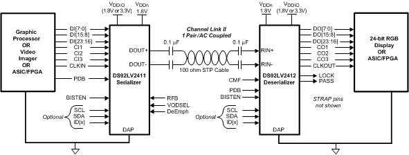
3.1 Typical Application Schematic