SNOSCY5B August 2014 – April 2015 FDC1004
PRODUCTION DATA.
- 1 Features
- 2 Applications
- 3 Description
- 4 Typical Application
- 5 Revision History
- 6 Pin Configuration and Functions
- 7 Specifications
- 8 Detailed Description
- 9 Applications and Implementation
- 10Power Supply Recommendations
- 11Layout
- 12Device and Documentation Support
- 13Mechanical, Packaging, and Orderable Information
パッケージ・オプション
メカニカル・データ(パッケージ|ピン)
サーマルパッド・メカニカル・データ
- DSC|10
発注情報
8 Detailed Description
8.1 Overview
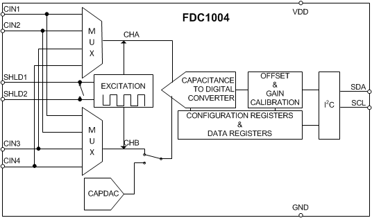
The FDC1004 is a high-resolution, 4-channel capacitance-to-digital converter for implementing capacitive sensing solutions. Each channel has a full scale range of ±15 pF and can handle a sensor offset capacitance of up to 100 pF, which can be either programmed internally or can be an external capacitor for tracking environmental changes over time and temperature. The large offset capacitance capability allows for the use of remote sensors. The FDC1004 also includes shield drivers for sensor shields, which can reduce EMI interference and help focus the sensing direction of a capacitive sensor. The small footprint of the FDC1004 allows for use in space-constrained applications. For more information on the basics of capacitive sensing and applications, refer to FDC1004: Basics of Capacitive Sensing and Applications application note (SNOA927).
8.2 Functional Block Diagram

8.3 Feature Description
8.3.1 The Shield
The FDC1004 measures capacitance between CINn and ground. That means any capacitance to ground on signal path between the FDC1004 CINn pins and sensor is included in the FDC1004 conversion result.
In some applications, the parasitic capacitance of the sensor connections can be larger than the capacitance of the sensor. If that parasitic capacitance is stable, it can be treated as a constant capacitive offset. However, the parasitic capacitance of the sensor connections can have significant variation due to environmental changes (such as mechanical movement, temperature shifts, humidity changes). These changes are seen as drift in the conversion result and may significantly compromise the system accuracy.
To eliminate the CINn parasitic capacitance to ground, the FDC1004 SHLDx signals can be used for shielding the connection between the sensor and CINn. The SHLDx output is the same signal waveform as the excitation of the CINn pin; the SHLDx is driven to the same voltage potential as the CINn pin. Therefore, there is no current between CINn and SHLDx pins, and any capacitance between these pins does not affect the CINn charge transfer. Ideally, the CINn to SHLD capacitance does not have any contribution to the FDC1004 result.
In differential measurements, SHLD1 is assigned to CHn and SHLD2 is assigned to CHm, where n < m. For instance in the measurement CIN1 – CIN2, where CHA = CIN1 and CHB = CIN2 (see Table 4), SHDL1 is assigned to CIN1 and SHDL2 is assigned to CIN2.
In a single ended configuration, such as CINn vs. GND, SHLD1 is internally shorted to SHLD2. In a single ended configuration, such as CINn vs. GND with CAPDAC enabled, SHLD1 is assigned to the selected channel, SHLD2 is floating.
For best results, locate the FDC1004 as close as possible to the capacitive sensor. Minimize the connection length between the sensor and FDC1004 CINn pins and between the sensor ground and the FDC1004 GND pin. Shield the PCB traces to the CINn pins and connect the shielding to the FDC1004 SHLDx pins. In addition, if a shielded cable is used to connect the FDC1004 to the sensor, the shield should be connected to the appropriate SHLDx pin. In applications where only one SHLDx pin is used, the unused SHLDx pin can be left unconnected.
For more information on shielding, refer to Capacitive Sensing: Ins and Outs of Active Sensing application note (SNOA926).
8.3.2 The CAPDAC
The FDC1004 full-scale input range is ±15 pF. The part can accept a higher capacitance on the input and the common-mode or offset (constant component) capacitance can be balanced by the programmable on-chip CAPDACs. The CAPDAC can be viewed as a negative capacitance connected internally to the CINn pin. The relation between the input capacitance and output data can be expressed as DATA = (CINn – CAPDAC), n = 1...4. The CAPDACs have a 5-bit resolution, monotonic transfer function, are well matched to each other, and have a defined temperature coefficient.
8.3.3 Capacitive System Offset Calibration
The capacitive offset can be due to many factors including the initial capacitance of the sensor, parasitic capacitances of board traces, and the capacitance of any other connections between the sensor and the FDC.
The parasitic capacitances of the FDC1004 are calibrated out at production. If there are other sources of offset in the system, it may be necessary to calibrate the system capacitance offset in the application. Any offset in the capacitance input larger than ½ LSB of the CAPDAC should first be removed using the on-chip CAPDACs. Any residual offset of approximately 1 pF can then be removed by using the capacitance offset calibration register. The offset calibration register is reloaded by the default value at power-on or after reset. Therefore, if the offset calibration is not repeated after each system power-up, the calibration coefficient value should be stored by the host controller and reloaded as part of the FDC1004 setup.
8.3.4 Capacitive Gain Calibration
The gain is factory calibrated up to ±15 pF in the production for each part individually. The factory gain coefficient is stored in a one-time programmable (OTP) memory.
The gain can be temporarily changed by setting the Gain Calibration Register (registers 0x11 to 0x14) for the appropriate CINn pin, although the factory gain coefficient will be restored after power-up or reset.
The part is tested and specified for use only with the default factory calibration coefficient. Adjusting the Gain calibration can be used to normalize the capacitance measurement of the CINn input channels.
8.4 Device Functional Modes
8.4.1 Single Ended Measurement
The FDC1004 can be used for interfacing to a single-ended capacitive sensor. In this configuration the sensor should be connected to the input CINn (n = 1..4) pins of the FDC1004 and GND. The capacitance-to-digital convertor (without using the CAPDAC, CAPDAC= 0pF) measures the positive (or the negative) input capacitance in the range of 0 pF to 15 pF. The CAPDAC can be used for programmable shifting of the input range. In this case it is possible to measure input capacitance in the range of 0 pF to ±15 pF which are on top of an offset capacitance up to 100 pF. In single ended measurements with CAPDAC disabled SHLD1 is internally shorted to SHLD2 (see Figure 10); if CAPDAC is enabled SHLD2 is floating (see Figure 11). The single ended mode is enabled when the CHB register of the Measurements configuration registers (see Table 4) are set to b100 or b111.
 Figure 10. Single-Ended Configuration with CAPDAC Disabled
 Figure 11. Single-Ended Configuration with CAPDAC Enabled
8.4.2 Differential Measurement
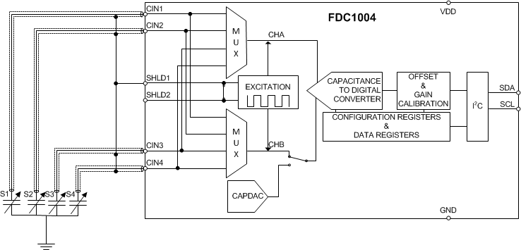
When the FDC1004 is used for interfacing to a differential capacitive sensor, each of the two input capacitances must be less than 115 pF. In this configuration the CAPDAC is disabled. The absolute value of the difference between the two input capacitances should be kept below 15 pF to avoid introducing errors in the measurement. In differential measurements, SHLD1 is assigned to CHn and SHLD2 is assigned to CHm, where n < m. For instance in the measurement CIN1 – CIN2, where CHA = CIN1 and CHB = CIN2 (see Table 4), SHDL1 is assigned to CIN1 and SHDL2 is to CIN2. Differential sensors made with S1 versus S3 and S2 versus S4 is shown below in Figure 12. S1 and S2 are alternatively connected to CHA and the S3 and S4 are alternatively connected to CHB, the shield signals are connected as explained in previous paragraph. The FDC1004 will perform a differential measurement when CHB field of the Measurements Configuration Registers (refer to Table 4) is less than to b100.
This configuration is very useful in applications where environment conditions need to be tracked. The differential measurement between the main electrode and the environment electrode makes the measurement independent of the environment conditions.
 Figure 12. Differential Configuration
8.5 Programming
The FDC1004 operates only as a slave device on the two-wire bus interface. Every device on the bus must have a unique address. Connection to the bus is made via the open-drain I/O lines, SDA, and SCL. The SDA and SCL pins feature integrated spike-suppression filters and Schmitt triggers to minimize the effects of input spikes and bus noise. The FDC1004 supports fast mode frequencies 10 kHz to 400 kHz. All data bytes are transmitted MSB first.
8.5.1 Serial Bus Address
To communicate with the FDC1004, the master must first address slave devices via a slave address byte. The slave address byte consists of seven address bits and a direction bit that indicates the intent to execute a read or write operation. The seven bit address for the FDC1004 is (MSB first): b101 0000.
8.5.2 Read/Write Operations
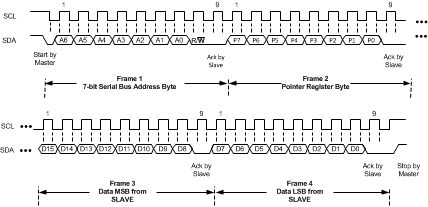
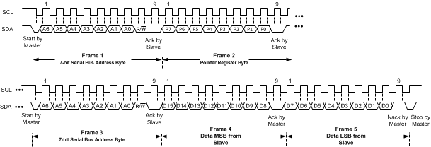
Access a particular register on the FDC1004 by writing the appropriate value to the Pointer Register. The pointer value is the first byte transferred after the slave address byte with the R/W bit low. Every write operation to the FDC1004 requires a value for the pointer register. When reading from the FDC1004, the last value stored in the pointer by a write operation is used to determine which register is read by a read operation. To change the pointer register for a read operation, a new value must be written to the pointer. This transaction is accomplished by issuing the slave address byte with the R/W bit low, followed by the pointer byte. No additional data is required. The master can then generate a START condition and send the slave address byte with the R/W bit high to initiate the read command. Note that register bytes are sent MSB first, followed by the LSB. A write operation in a read only registers such as MANUFACTURER ID or SERIAL ID returns a NACK after each data byte; read/write operation to unused address returns a NACK after the pointer; a read/write operation with incorrect I2C address returns a NACK after the I2C address.
 Figure 13. Write Frame
 Figure 14. Read Frame
8.5.3 Device Usage
The basic usage model of the FDC1004 is to simply follow these steps:
- Configure measurements (for details, refer to Measurement Configuration).
- Trigger a measurement set (for details, refer to Triggering Measurements).
- Wait for measurement completion (for details, refer to Wait for Measurement Completion).
- Read measurement data (for details, refer to Read of Measurement Result).
8.5.3.1 Measurement Configuration
Configuring a measurement involves setting the input channels and the type of measurement (single-ended or differential).
The FDC1004 can be configured with up to 4 separate measurements, where each measurement can be any valid configuration (that is, a specific channel can be used in multiple measurements). There is a dedicated configuration register for each of the 4 possible measurements (e.g MEAS_CONF1 in register 0x08 configures measurement 1, MEAS_CONF2 in register 0x09 configures measurement 2, ...). Configuring only one measurement is allowed, and it can be one of the 4 possible measurement configurations.
- Setup the input channels for each measurement. Determine which of the 4 measurement configuration registers to use (registers 0x08 to 0x0A) and set the following:
- For single-ended measurement:
- Select the positive input pin for the measurement by setting the CHA field (bits[15:13]).
- Set CAPDAC (bits[9:5]) if the channel offset capacitance is more than 15pF.
- For a differential measurement:
- Select the positive input pin for the measurement by setting the CHA field (bits[15:13]).
- Select the negative input pin for the measurement by setting the CHB field (bits[12:10]). Note that the CAPDAC setting has no effect for a differential measurement.
- For single-ended measurement:
- Determine the appropriate sample rate. The sample rate sets the resolution of the measurement. Lower the sample rate higher is the resolution of the measurement.
8.5.3.2 Triggering Measurements
For a single measurement, trigger the desired measurement (i.e. which one of the configured measurements) when needed by:
- Setting REPEAT (Register 0x0C:bit[8]) to 0.
- Setting the corresponding MEAS_x field (Register 0x0C:bit[7:4]) to 1.
- For example, to trigger a single measurement of Measurement 2 at a rate of 100S/s, set Address 0x0C to 0x0540.
The FDC1004 can also trigger a new measurement on the completion of the previous measurement (repeated measurements). This is setup by:
- Setting REPEAT (Register 0x0C:bit[8]) to 1.
- Setting the corresponding MEAS_x field (Register 0x0C:bit[7:4]) to 1.
8.5.3.3 Wait for Measurement Completion
Wait for the triggered measurements to complete. When the measurements are complete, the corresponding DONE_x field (Register 0x0C:bits[3:0]) will be set to 1.
8.5.3.4 Read of Measurement Result
Read the result of the measurement from the corresponding registers:
- 0x00/0x01 for Measurement 1
- 0x02/0x03 for Measurement 2
- 0x04/0x05 for Measurement 3
- 0x06/0x07 for Measurement 4
Once the measurement read is complete, the corresponding DONE_x field (Register 0x0C:bits[3:0]) will return to 0.
If an additional single triggered measurement is desired, simply perform the Trigger, Wait, Read steps again.
If the FDC1004 is setup for repeated measurements (Register 0x0C:bit[8]) = 1), the FDC1004 will continuously measure until the REPEAT field (Register 0x0C:bit[8]) is set to 0, even if the results are not read back.
8.6 Register Maps
Table 1. Register Map
| Pointer | Register Name | Reset Value | Description |
|---|---|---|---|
| 0x00 | MEAS1_MSB | 0x0000 | MSB portion of Measurement 1 |
| 0x01 | MEAS1_LSB | 0x0000 | LSB portion of Measurement 1 |
| 0x02 | MEAS2_MSB | 0x0000 | MSB portion of Measurement 2 |
| 0x03 | MEAS2_LSB | 0x0000 | LSB portion of Measurement 2 |
| 0x04 | MEAS3_MSB | 0x0000 | MSB portion of Measurement 3 |
| 0x05 | MEAS3_LSB | 0x0000 | LSB portion of Measurement 3 |
| 0x06 | MEAS4_MSB | 0x0000 | MSB portion of Measurement 4 |
| 0x07 | MEAS4_LSB | 0x0000 | LSB portion of Measurement 4 |
| 0x08 | CONF_MEAS1 | 0x1C00 | Measurement 1 Configuration |
| 0x09 | CONF_MEAS2 | 0x1C00 | Measurement 2 Configuration |
| 0x0A | CONF_MEAS3 | 0x1C00 | Measurement 3 Configuration |
| 0x0B | CONF_MEAS4 | 0x1C00 | Measurement 4 Configuration |
| 0x0C | FDC_CONF | 0x0000 | Capacitance to Digital Configuration |
| 0x0D | OFFSET_CAL_CIN1 | 0x0000 | CIN1 Offset Calibration |
| 0x0E | OFFSET_CAL_CIN2 | 0x0000 | CIN2 Offset Calibration |
| 0x0F | OFFSET_CAL_CIN3 | 0x0000 | CIN3 Offset Calibration |
| 0x10 | OFFSET_CAL_CIN4 | 0x0000 | CIN4 Offset Calibration |
| 0x11 | GAIN_CAL_CIN1 | 0x4000 | CIN1 Gain Calibration |
| 0x12 | GAIN_CAL_CIN2 | 0x4000 | CIN2 Gain Calibration |
| 0x13 | GAIN_CAL_CIN3 | 0x4000 | CIN3 Gain Calibration |
| 0x14 | GAIN_CAL_CIN4 | 0x4000 | CIN4 Gain Calibration |
| 0xFE | Manufacturer ID | 0x5449 | ID of Texas Instruments |
| 0xFF | Device ID | 0x1004 | ID of FDC1004 device |
Registers from 0x15 to 0xFD are reserved and should not be written to.
8.6.1 Registers
The FDC1004 has an 8-bit pointer used to address a given data register. The pointer identifies which of the data registers should respond to a read or write command on the two-wire bus. This register is set with every write command. A write command must be issued to set the proper value in the pointer before executing a read command. The power-on reset (POR) value of the pointer is 0x00.
8.6.1.1 Capacitive Measurement Registers
The capacitance measurement registers are 24-bit result registers in binary format (the 8 LSBs D[7:0] are always 0x00). The result of the acquisition is always a 24 bit value, while the accuracy is related to the selected conversion time (refer to Electrical Characteristicsnote to Electrical Characteristics table). The data is encoded in a Two’s complement format. The result of the measurement can be calculated by the following formula:
where
- Coffset is based on the CAPDAC setting.
Table 2. Measurement Registers Description (0x00, 0x02, 0x04, 0x06)
| Field Name | Bits | Description | ||
|---|---|---|---|---|
| MSB_MEASn(1) | [15:0] | Most significant 16 bits of Measurement n (read only) | ||
Table 3. Measurement Registers Description (0x01, 0x03, 0x05, 0x07)
| Field Name | Bits | Description | ||
|---|---|---|---|---|
| LSB_MEASn(1) | [15:8] | Least significant 8 bits of Measurement n (read only) | ||
| [7:0] | Reserved | Reserved, always 0 (read only) | ||
8.6.2 Measurement Configuration Registers
These registers configure the input channels and CAPDAC setting for a measurement.
Table 4. Measurement Configuration Registers Description (0x08, 0x09, 0x0A, 0x0B)
| Field Name | Bits | Description | ||
|---|---|---|---|---|
| CHA(1)(2) | [15:13] | Positive input channel capacitive to digital converter | b000 | CIN1 |
| b001 | CIN2 | |||
| b010 | CIN3 | |||
| b011 | CIN4 | |||
| CHB(1)(2) | [12:10] | Negative input channel capacitive to digital converter | b000 | CIN1 |
| b001 | CIN2 | |||
| b010 | CIN3 | |||
| b011 | CIN4 | |||
| b100 | CAPDAC | |||
| b111 | DISABLED | |||
| CAPDAC | [9:5] | Offset Capacitance | b00000 | 0pF (minimum programmable offset) |
| - - - - - | Configure the single-ended measurement capacitive offset: Coffset = CAPDAC x 3.125pF |
|||
| b11111 | 96.875pF (maximum programmable offset) | |||
| RESERVED | [04:00] | Reserved | Reserved, always 0 (read only) | |
8.6.3 FDC Configuration Register
This register configures measurement triggering and reports measurement completion.
Table 5. FDC Register Description (0x0C)
| Field Name | Bits | Description | ||
|---|---|---|---|---|
| RST | [15] | Reset | 0 | Normal operation |
| 1 | Software reset: write a 1 to initiate a device reset; after completion of reset this field will return to 0 | |||
| RESERVED | [14:12] | Reserved | Reserved, always 0 (read only) | |
| RATE | [11:10] | Measurement Rate | b00 | Reserved |
| b01 | 100S/s | |||
| b10 | 200S/s | |||
| b11 | 400S/s | |||
| RESERVED | [9] | Reserved | Reserved, always 0 (read only) | |
| REPEAT | [8] | Repeat Measurements | 0 | Repeat disabled |
| 1 | Repeat enabled, all the enabled measurement are repeated | |||
| MEAS_1 | [7] | Initiate Measurements | 0 | Measurement 1 disabled |
| 1 | Measurement 1 enabled | |||
| MEAS_2 | [6] | Initiate Measurements | 0 | Measurement 2 disabled |
| 1 | Measurement 2 enabled | |||
| MEAS_3 | [5] | Initiate Measurements | 0 | Measurement 3 disabled |
| 1 | Measurement 3 enabled | |||
| MEAS_4 | [4] | Initiate Measurements | 0 | Measurement 4 disabled |
| 1 | Measurement 4 enabled | |||
| DONE_1 | [3] | Measurement Done | 0 | Measurement 1 not completed |
| 1 | Measurement 1 completed | |||
| DONE_2 | [2] | Measurement Done | 0 | Measurement 2 not completed |
| 1 | Measurement 2 completed | |||
| DONE_3 | [1] | Measurement Done | 0 | Measurement 3 not completed |
| 1 | Measurement 3 completed | |||
| DONE_4 | [0] | Measurement Done | 0 | Measurement 4 not completed |
| 1 | Measurement 4 completed | |||
8.6.4 Offset Calibration Registers
These registers configure a digitized capacitance value in the range of -16 pF to 16 pF (max residual offset 250 aF) that can be added to each channel in order to remove parasitic capacitance due to external circuitry. In addition to the offset calibration capacitance which is a fine-tune offset capacitance, it is possible to support a larger offset by using the CAPDAC (for up to 100 pF). These 16-bit registers are formatted as a fixed point number, where the first 5 bits represents the integer portion of the capacitance in Two’s complement format, and the remaining 11 bits represent the fractional portion of the capacitance.
Table 6. Offset Calibration Registers Description (0x0D, 0x0E, 0x0F, 0x10)
| Field Name | Bits | Description | ||
|---|---|---|---|---|
| OFFSET_CALn(1) | [15:11] | Integer part | Integer portion of the Offset Calibration of Channel CINn | |
| [10:0] | Decimal part | Decimal portion of the Offset Calibration of Channel CINn | ||
8.6.5 Gain Calibration Registers
These registers contain a gain factor correction in the range of 0 to 4 that can be applied to each channel in order to remove gain mismatch due to the external circuitry. This 16-bit register is formatted as a fixed point number, where the 2 MSBs of the GAIN_CALn register correspond to an integer portion of the gain correction, and the remaining 14 bits represent the fractional portion of the gain correction. The result of the conversion represents a number without dimensions.
The Gain can be set according to the following formula:
Gain = GAIN_CAL[15:0]/214
Table 7. Gain Calibration Registers Description (0x11, 0x12, 0x13, 0x14)
| Field Name | Bits | Description | ||
|---|---|---|---|---|
| GAIN_CALn(1) | [15:14] | Integer part | Integer portion of the Gain Calibration of Channel CINn | |
| [13:0] | Decimal part | Decimal portion of the Gain Calibration of Channel CINn | ||
8.6.6 Manufacturer ID Register
This register contains a factory-programmable identification value that identifies this device as being manufactured by Texas Instruments. This register distinguishes this device from other devices that are on the same I2C bus. The manufacturer ID reads 0x5449.
Table 8. Manufacturer ID Register Description (0xFE)
| Field Name | Bits | Description | ||
|---|---|---|---|---|
| MANUFACTURER ID | [15:0] | Manufacturer ID | 0x5449h | Texas instruments ID (read only) |
8.6.7 Device ID Register
This register contains a factory-programmable identification value that identifies this device as a FDC1004. This register distinguishes this device from other devices that are on the same I2C bus. The Device ID for the FDC1004 is 0x1004.
Table 9. Device ID Register Description (0xFF)
| Field Name | Bits | Description | ||
|---|---|---|---|---|
| DEVICE ID | [15:0] | Device ID | 0x1004 | FDC1004 Device ID (read only) |