SBOS547A June 2011 – August 2015 INA226
PRODUCTION DATA.
- 1 Features
- 2 Applications
- 3 Description
- 4 Revision History
- 5 Pin Configuration and Functions
- 6 Specifications
-
7 Detailed Description
- 7.1 Overview
- 7.2 Functional Block Diagram
- 7.3 Feature Description
- 7.4 Device Functional Modes
- 7.5 Programming
- 7.6
Register Maps
- 7.6.1 Configuration Register (00h) (Read/Write)
- 7.6.2 Shunt Voltage Register (01h) (Read-Only)
- 7.6.3 Bus Voltage Register (02h) (Read-Only)
- 7.6.4 Power Register (03h) (Read-Only)
- 7.6.5 Current Register (04h) (Read-Only)
- 7.6.6 Calibration Register (05h) (Read/Write)
- 7.6.7 Mask/Enable Register (06h) (Read/Write)
- 7.6.8 Alert Limit Register (07h) (Read/Write)
- 7.6.9 Manufacturer ID Register (FEh) (Read-Only)
- 7.6.10 Die ID Register (FFh) (Read-Only)
- 8 Application and Implementation
- 9 Power Supply Recommendations
- 10Layout
- 11Device and Documentation Support
- 12Mechanical, Packaging, and Orderable Information
6 Specifications
6.1 Absolute Maximum Ratings
over operating free-air temperature range (unless otherwise noted) (1)| MIN | MAX | UNIT | ||
|---|---|---|---|---|
| VVS | Supply voltage | 6 | V | |
| Analog Inputs, IN+, IN– | Differential (VIN+ – VIN-)(2) | –40 | 40 | V |
| Common-Mode (VIN+ + VIN-) / 2 | –0.3 | 40 | ||
| VVBUS | –0.3 | 40 | V | |
| VSDA | GND – 0.3 | 6 | V | |
| VSCL | GND – 0.3 | VVS + 0.3 | V | |
| IIN | Input current into any pin | 5 | mA | |
| IOUT | Open-drain digital output current | 10 | mA | |
| TJ | Junction temperature | 150 | °C | |
| Tstg | Storage temperature range | –65 | 150 | °C |
(1) Stresses beyond those listed under Absolute Maximum Ratings may cause permanent damage to the device. These are stress ratings only, which do not imply functional operation of the device at these or any other conditions beyond those indicated under Recommended Operating Conditions. Exposure to absolute-maximum-rated conditions for extended periods may affect device reliability.
(2) IN+ and IN– may have a differential voltage between –40 V and 40 V. However, the voltage at these pins must not exceed the range –0.3 V to 40 V.
6.2 ESD Ratings
| VALUE | UNIT | |||
|---|---|---|---|---|
| V(ESD) | Electrostatic discharge | Human body model (HBM), per ANSI/ESDA/JEDEC JS-001, all pins(1) | ±2500 | V |
| Charged device model (CDM), per JEDEC specification JESD22-C101, all pins(2) | ±1000 | |||
| Machine model (MM) | ±150 | |||
(1) JEDEC document JEP155 states that 500-V HBM allows safe manufacturing with a standard ESD control process.
(2) JEDEC document JEP157 states that 250-V CDM allows safe manufacturing with a standard ESD control process.
6.3 Recommended Operating Conditions
over operating free-air temperature range (unless otherwise noted)| MIN | NOM | MAX | UNIT | ||
|---|---|---|---|---|---|
| VCM | Common-mode input voltage | 12 | V | ||
| VVS | Operating supply voltage | 3.3 | V | ||
| TA | Operating free-air temperature | –40 | 125 | °C | |
6.4 Thermal Information
| THERMAL METRIC(1) | INA226 | UNIT | |
|---|---|---|---|
| DGS (VSSOP) | |||
| 10 PINS | |||
| RθJA | Junction-to-ambient thermal resistance | 171.4 | °C/W |
| RθJC(top) | Junction-to-case (top) thermal resistance | 42.9 | °C/W |
| RθJB | Junction-to-board thermal resistance | 91.8 | °C/W |
| ψJT | Junction-to-top characterization parameter | 1.5 | °C/W |
| ψJB | Junction-to-board characterization parameter | 90.2 | °C/W |
| RθJC(bot) | Junction-to-case (bottom) thermal resistance | n/a | °C/W |
(1) For more information about traditional and new thermal metrics, see the Semiconductor and IC Package Thermal Metrics application report, SPRA953.
6.5 Electrical Characteristics
TA = 25°C, VVS = 3.3 V, VIN+ = 12 V, VSENSE = (VIN+ – VIN–) = 0 mV and VVBUS = 12 V, unless otherwise noted| PARAMETER | TEST CONDITIONS | MIN | TYP | MAX | UNIT | |
|---|---|---|---|---|---|---|
| INPUT | ||||||
| Shunt voltage input range | –81.9175 | 81.92 | mV | |||
| Bus voltage input range(1) | 0 | 36 | V | |||
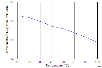
| CMRR | Common-mode rejection | 0 V ≤ VIN+ ≤ 36 V | 126 | 140 | dB | |
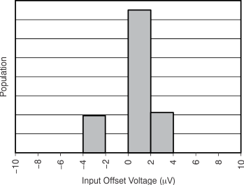
| VOS | Shunt offset voltage, RTI(2) | ±2.5 | ±10 | μV | ||
| Shunt offset voltage, RTI(2) vs temperature | –40°C ≤ TA ≤ 125°C | 0.02 | 0.1 | μV/°C | ||
| PSRR | Shunt offset voltage, RTI(2) vs Power supply | 2.7 V ≤ VS ≤ 5.5 V | 2.5 | μV/V | ||
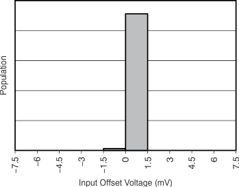
| VOS | Bus offset voltage, RTI(2) | ±1.25 | ±7.5 | mV | ||
| Bus offset voltage, RTI(2) vs temperature | –40°C ≤ TA ≤ 125°C | 10 | 40 | μV/°C | ||
| PSRR | Bus offset voltage, RTI(2) vs power supply | 0.5 | mV/V | |||
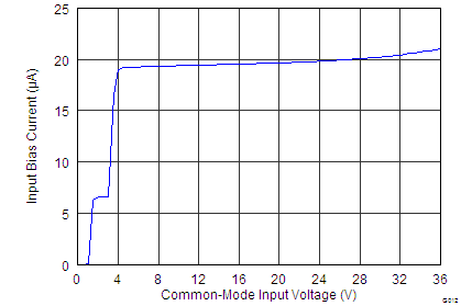
| IB | Input bias current (IIN+, IIN– pins) | 10 | μA | |||
| VBUS input impedance | 830 | kΩ | ||||
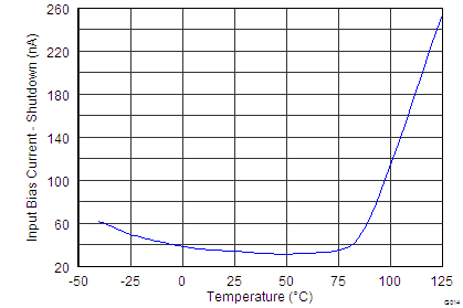
| Input leakage (3) | (IN+ pin) + (IN– pin), Power-down mode |
0.1 | 0.5 | μA | ||
| DC ACCURACY | ||||||
| ADC native resolution | 16 | Bits | ||||
| 1 LSB step size | Shunt voltage | 2.5 | μV | |||
| Bus voltage | 1.25 | mV | ||||
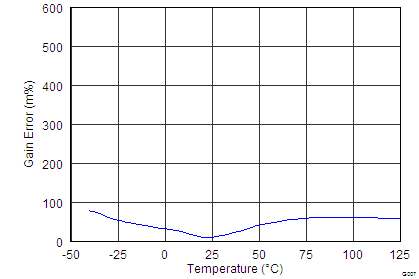
| Shunt voltage gain error | 0.02% | 0.1% | ||||
| Shunt voltage gain error vs temperature | –40°C ≤ TA ≤ 125°C | 10 | 50 | ppm/°C | ||
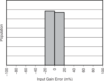
| Bus voltage gain error | 0.02% | 0.1% | ||||
| Bus voltage gain error vs temperature | –40°C ≤ TA ≤ 125°C | 10 | 50 | ppm/°C | ||
| Differential nonlinearity | ±0.1 | LSB | ||||
| tCT | ADC conversion time | CT bit = 000 | 140 | 154 | μs | |
| CT bit = 001 | 204 | 224 | ||||
| CT bit = 010 | 332 | 365 | ||||
| CT bit = 011 | 588 | 646 | ||||
| CT bit = 100 | 1.1 | 1.21 | ms | |||
| CT bit = 101 | 2.116 | 2.328 | ||||
| CT bit = 110 | 4.156 | 4.572 | ||||
| CT bit = 111 | 8.244 | 9.068 | ||||
| SMBus | ||||||
| SMBus timeout(4) | 28 | 35 | ms | |||
| DIGITAL INPUT/OUTPUT | ||||||
| Input capacitance | 3 | pF | ||||
| Leakage input current | 0 V ≤ VSCL ≤ VVS , 0 V ≤ VSDA ≤ VVS, 0 V ≤ VAlert ≤ VVS , 0 V ≤ VA0 ≤ VVS , 0 V ≤ VA1 ≤ VVS |
0.1 | 1 | μA | ||
| VIH | High-level input voltage | 0.7×VVS | 6 | V | ||
| VIL | Low-level input voltage | –0.5 | 0.3×VVS | V | ||
| VOL | Low-level output voltage, SDA, Alert | IOL = 3 mA | 0 | 0.4 | V | |
| Hysteresis | 500 | mV | ||||
| POWER SUPPLY | ||||||
| Operating supply range | 2.7 | 5.5 | V | |||
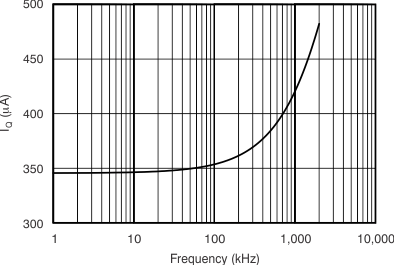
| IQ | Quiescent current | 330 | 420 | μA | ||
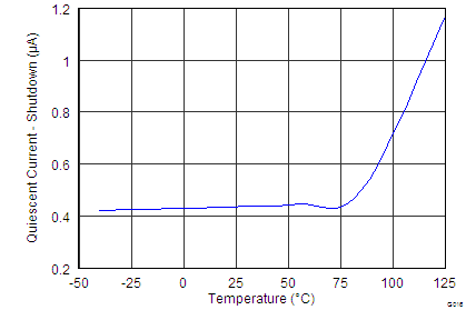
| Quiescent current, power-down (shutdown) mode | 0.5 | 2 | μA | |||
| VPOR | Power-on reset threshold | 2 | V | |||
(1) While the input range is 36 V, the full-scale range of the ADC scaling is 40.96 V. See the Basic ADC Functions section. Do not apply more than 36 V.
(2) RTI = Referred-to-input.
(3) Input leakage is positive (current flowing into the pin) for the conditions shown at the top of this table. Negative leakage currents can occur under different input conditions.
(4) SMBus timeout in the INA226 resets the interface any time SCL is low for more than 28 ms.
6.6 Typical Characteristics
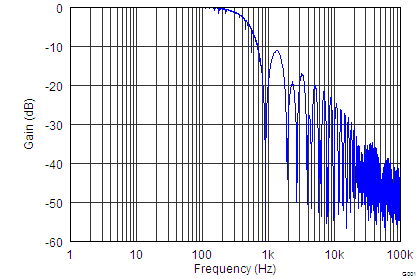
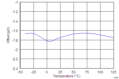
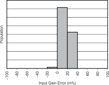
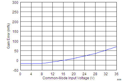
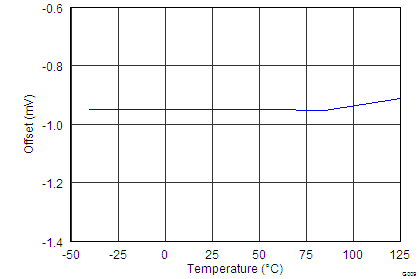
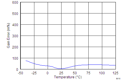
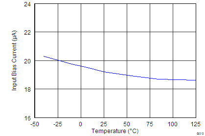
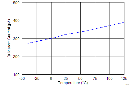
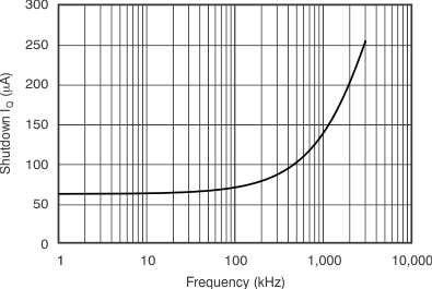
At TA = 25°C, VVS = 3.3 V, VIN+ = 12 V, VSENSE = (VIN+ – VIN–) = 0 mV and VVBUS = 12 V, unless otherwise noted.