JAJSDX8E June 2017 – August 2018 ISO1211 , ISO1212
PRODUCTION DATA.
- 1 特長
- 2 アプリケーション
- 3 概要
- 4 改訂履歴
- 5 概要(続き)
- 6 Pin Configuration and Functions
-
7 Specifications
- 7.1 Absolute Maximum Ratings
- 7.2 ESD Ratings
- 7.3 Recommended Operating Conditions
- 7.4 Thermal Information
- 7.5 Power Ratings
- 7.6 Insulation Specifications
- 7.7 Safety-Related Certifications
- 7.8 Safety Limiting Values
- 7.9 Electrical Characteristics—DC Specification
- 7.10 Switching Characteristics—AC Specification
- 7.11 Insulation Characteristics Curves
- 7.12 Typical Characteristics
- 8 Parameter Measurement Information
- 9 Detailed Description
-
10Application and Implementation
- 10.1 Application Information
- 10.2
Typical Application
- 10.2.1
Sinking Inputs
- 10.2.1.1 Design Requirements
- 10.2.1.2
Detailed Design Procedure
- 10.2.1.2.1 Setting Current Limit and Voltage Thresholds
- 10.2.1.2.2 Thermal Considerations
- 10.2.1.2.3 Designing for 48-V Systems
- 10.2.1.2.4 Designing for Input Voltages Greater Than 60 V
- 10.2.1.2.5 Surge, ESD, and EFT Tests
- 10.2.1.2.6 Multiplexing the Interface to the Host Controller
- 10.2.1.2.7 Status LEDs
- 10.2.1.3 Application Curve
- 10.2.2 Sourcing Inputs
- 10.2.3 Sourcing and Sinking Inputs (Bidirectional Inputs)
- 10.2.1
Sinking Inputs
- 11Power Supply Recommendations
- 12Layout
- 13デバイスおよびドキュメントのサポート
- 14メカニカル、パッケージ、および注文情報
パッケージ・オプション
デバイスごとのパッケージ図は、PDF版データシートをご参照ください。
メカニカル・データ(パッケージ|ピン)
- D|8
サーマルパッド・メカニカル・データ
発注情報
10.2.1 Sinking Inputs
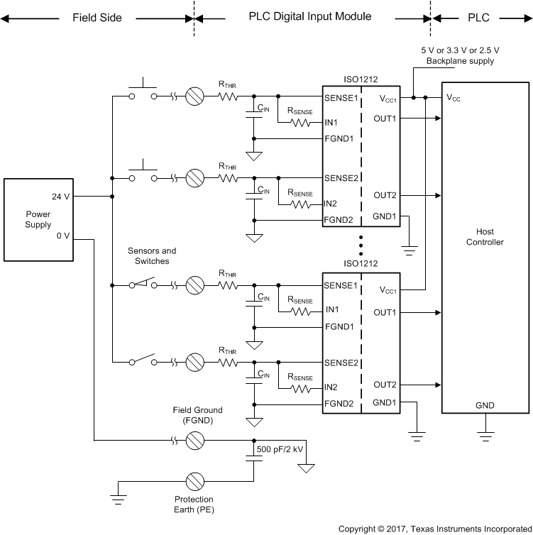
Figure 16 shows the design for a typical multichannel, isolated digital-input module with sinking inputs. Push-button switches, proximity sensors, and other field inputs connect to the host controller through an isolated interface. The design is easily scalable from a few channels, such as 4 or 8, to many channels, such as 256 or more. The RSENSE resistor limits the current drawn from the input pins. The RTHR resistor is used to adjust the voltage thresholds and limit the peak current during surge events. The CIN capacitor is used to filter noise on the input pins. For more information on selecting RSENSE, RTHR, and CIN, see the Detailed Design Procedure section.
The ISO121x devices derive field-side power from the input pins which eliminates the requirement for a field-side, 24-V input power supply to the module. Similarly, an isolated dc-dc converter creating a field-side power supply from the controller side back plane supply is also eliminated which improves flexibility of system design and reduces system cost.
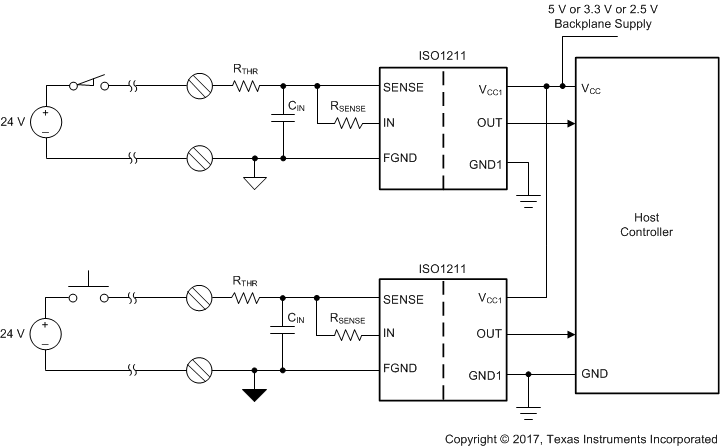
For systems requiring channel-to-channel isolation on the field side, use the ISO1211 device as shown in Figure 17.
 Figure 16. Typical Application Schematic With Sinking Inputs
  Figure 17. Single-Channel or Channel-to-Channel Isolated Designs With ISO1211