JAJSDX8E June 2017 – August 2018 ISO1211 , ISO1212
PRODUCTION DATA.
- 1 特長
- 2 アプリケーション
- 3 概要
- 4 改訂履歴
- 5 概要(続き)
- 6 Pin Configuration and Functions
-
7 Specifications
- 7.1 Absolute Maximum Ratings
- 7.2 ESD Ratings
- 7.3 Recommended Operating Conditions
- 7.4 Thermal Information
- 7.5 Power Ratings
- 7.6 Insulation Specifications
- 7.7 Safety-Related Certifications
- 7.8 Safety Limiting Values
- 7.9 Electrical Characteristics—DC Specification
- 7.10 Switching Characteristics—AC Specification
- 7.11 Insulation Characteristics Curves
- 7.12 Typical Characteristics
- 8 Parameter Measurement Information
- 9 Detailed Description
-
10Application and Implementation
- 10.1 Application Information
- 10.2
Typical Application
- 10.2.1
Sinking Inputs
- 10.2.1.1 Design Requirements
- 10.2.1.2
Detailed Design Procedure
- 10.2.1.2.1 Setting Current Limit and Voltage Thresholds
- 10.2.1.2.2 Thermal Considerations
- 10.2.1.2.3 Designing for 48-V Systems
- 10.2.1.2.4 Designing for Input Voltages Greater Than 60 V
- 10.2.1.2.5 Surge, ESD, and EFT Tests
- 10.2.1.2.6 Multiplexing the Interface to the Host Controller
- 10.2.1.2.7 Status LEDs
- 10.2.1.3 Application Curve
- 10.2.2 Sourcing Inputs
- 10.2.3 Sourcing and Sinking Inputs (Bidirectional Inputs)
- 10.2.1
Sinking Inputs
- 11Power Supply Recommendations
- 12Layout
- 13デバイスおよびドキュメントのサポート
- 14メカニカル、パッケージ、および注文情報
パッケージ・オプション
デバイスごとのパッケージ図は、PDF版データシートをご参照ください。
メカニカル・データ(パッケージ|ピン)
- D|8
サーマルパッド・メカニカル・データ
発注情報
10.2.1.2.5 Surge, ESD, and EFT Tests
Digital input modules are subject to surge (IEC 61000-4-5), electrostatic discharge or ESD (IEC 61000-4-2) and electrical fast transient or EFT (IEC 61000-4-4) tests. The surge impulse waveform has the highest energy and the widest pulse width, and is therefore the most stringent test of the three.
Figure 16 shows the application diagram for Type 1 and 3 systems. For a 1-kVPP surge test between the input terminals and protection earth (PE), a value of 1 kΩ for RTHR and 10 nF for CIN is recommended. Table 3 lists a summary of recommended component values to meet different levels of EMC requirements for Type 1 and 3 systems.
Table 3. Surge, IEC ESD and EFT
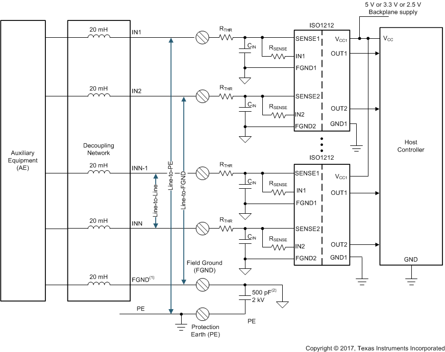
Figure 23 shows the test setup and application circuit used for surge testing. A noise filtering capacitor of 500 pF is recommended between the FGND pin and PE (earth). The total value of effective capacitance between the FGND pin and any other ground potential (including PE) must not exceed 500 pF for optimum surge performance. For line-to-PE test (common-mode test), the FGND pin is connected to the auxiliary equipment (AE) through a decoupling network.

For higher voltage levels of surge tests or for faster systems that cannot use a large value for CIN, TVS diodes or varistors can be used to meet EMC requirements. Type 2 systems that use a smaller value for RTHR may also require TVS diodes or varistors for surge protection. Figure 24 shows an example usage of TVS diodes for surge protection. The recommended components for surge protection are VCAN26A2-03S (TVS, Vishay), EZJ-P0V420WM (Varistor, Panasonic), and GSOT36C (TVS, Vishay).
Use of the RTHR resistor also reduces the peak current requirement for the TVS diodes, making them smaller and cost effective. For example, a 2-kV surge through a 1-kΩ RTHR resistor creates only 2-A peak current. Also, because of voltage drop across the RTHR resistor in normal operation, the working voltage requirement for the varistor or TVS diodes is reduced. For example, for a RTHR value of 1 kΩ and an RSENSE value of 562 Ω, a module designed for 30-V inputs only requires 28-V TVS diodes because the RTHR resistor drops more than 2 V.
 Figure 24. TVS Diodes Used Instead of a Filtering Capacitor for Surge Protection in Faster Systems