JAJSDX8E June 2017 – August 2018 ISO1211 , ISO1212
PRODUCTION DATA.
- 1 特長
- 2 アプリケーション
- 3 概要
- 4 改訂履歴
- 5 概要(続き)
- 6 Pin Configuration and Functions
-
7 Specifications
- 7.1 Absolute Maximum Ratings
- 7.2 ESD Ratings
- 7.3 Recommended Operating Conditions
- 7.4 Thermal Information
- 7.5 Power Ratings
- 7.6 Insulation Specifications
- 7.7 Safety-Related Certifications
- 7.8 Safety Limiting Values
- 7.9 Electrical Characteristics—DC Specification
- 7.10 Switching Characteristics—AC Specification
- 7.11 Insulation Characteristics Curves
- 7.12 Typical Characteristics
- 8 Parameter Measurement Information
- 9 Detailed Description
-
10Application and Implementation
- 10.1 Application Information
- 10.2
Typical Application
- 10.2.1
Sinking Inputs
- 10.2.1.1 Design Requirements
- 10.2.1.2
Detailed Design Procedure
- 10.2.1.2.1 Setting Current Limit and Voltage Thresholds
- 10.2.1.2.2 Thermal Considerations
- 10.2.1.2.3 Designing for 48-V Systems
- 10.2.1.2.4 Designing for Input Voltages Greater Than 60 V
- 10.2.1.2.5 Surge, ESD, and EFT Tests
- 10.2.1.2.6 Multiplexing the Interface to the Host Controller
- 10.2.1.2.7 Status LEDs
- 10.2.1.3 Application Curve
- 10.2.2 Sourcing Inputs
- 10.2.3 Sourcing and Sinking Inputs (Bidirectional Inputs)
- 10.2.1
Sinking Inputs
- 11Power Supply Recommendations
- 12Layout
- 13デバイスおよびドキュメントのサポート
- 14メカニカル、パッケージ、および注文情報
パッケージ・オプション
デバイスごとのパッケージ図は、PDF版データシートをご参照ください。
メカニカル・データ(パッケージ|ピン)
- D|8
サーマルパッド・メカニカル・データ
発注情報
6 Pin Configuration and Functions
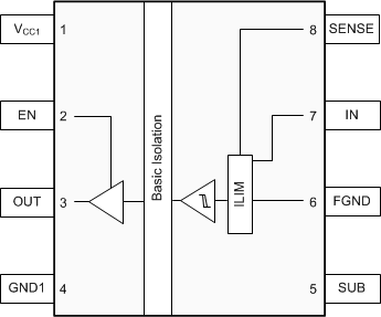
ISO1211 D Package
8-Pin SOIC
Top View

Pin Functions
| PIN | I/O | DESCRIPTION | |
|---|---|---|---|
| NO. | NAME | ||
| 1 | VCC1 | — | Power supply, side 1 |
| 2 | EN | I | Output enable. The output pin on side 1 is enabled when the EN pin is high or open. The output pin on side 1 is in the high-impedance state when the EN pin is low. In noisy applications, tie the EN pin to VCC1. |
| 3 | OUT | O | Channel output |
| 4 | GND1 | — | Ground connection for VCC1 |
| 5 | SUB | — | Internal connection to input chip substrate. Leave this pin unconnected on the board. |
| 6 | FGND | — | Field-side ground |
| 7 | IN | I | Field-side current input |
| 8 | SENSE | I | Field-side voltage sense |
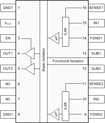
ISO1212 DBQ Package
16-Pin SSOP
Top View

Pin Functions
| PIN | I/O | Description | |
|---|---|---|---|
| NO. | NAME | ||
| 1 | GND1 | — | Ground connection for VCC1 |
| 2 | VCC1 | — | Power supply, side 1 |
| 3 | EN | I | Output enable. The output pins on side 1 are enabled when the EN pin is high or open. The output pins on side 1 are in the high-impedance state when the EN pin is low. In noisy applications, tie the EN pin to VCC1. |
| 4 | OUT1 | O | Channel 1 output |
| 5 | OUT2 | O | Channel 2 output |
| 6 | NC | — | Not connected |
| 7 | |||
| 8 | GND1 | — | Ground connection for VCC1 |
| 9 | FGND2 | — | Field-side ground, channel 2 |
| 10 | IN2 | I | Field-side current input, channel 2 |
| 11 | SENSE2 | I | Field-side voltage sense, channel 2 |
| 12 | SUB2 | — | Internal connection to input chip 2 substrate. Leave this pin unconnected on the board. |
| 13 | SUB1 | — | Internal connection to input chip 1 substrate. Leave this pin unconnected on the board. |
| 14 | FGND1 | — | Field-side ground, channel 1 |
| 15 | IN1 | I | Field-side current input, channel 1 |
| 16 | SENSE1 | I | Field-side voltage sense, channel 1 |