JAJSFM6A June 2018 – October 2018 ISO224
PRODUCTION DATA.
- 1 特長
- 2 アプリケーション
- 3 概要
- 4 改訂履歴
- 5 デバイス比較表
- 6 Pin Configuration and Functions
-
7 Specifications
- 7.1 Absolute Maximum Ratings
- 7.2 ESD Ratings
- 7.3 Recommended Operating Conditions
- 7.4 Thermal Information
- 7.5 Power Ratings
- 7.6 Insulation Specifications
- 7.7 Safety-Related Certifications
- 7.8 Safety Limiting Values
- 7.9 Electrical Characteristics
- 7.10 Switching Characteristics
- 7.11 Insulation Characteristics Curves
- 7.12 Typical Characteristics
- 8 Detailed Description
- 9 Application and Implementation
- 10Power Supply Recommendations
- 11Layout
- 12デバイスおよびドキュメントのサポート
- 13メカニカル、パッケージ、および注文情報
9.2.3 Application Curves
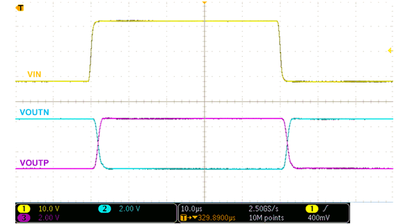
In some applications the system must be protected in case of an overvoltage condition. To allow for fast powering off of the system, a low delay caused by the isolated amplifier is required. Figure 49 shows the typical full-scale step response of the device. Consider the delay of the required window comparator and the MCU to calculate the overall response time of the system.

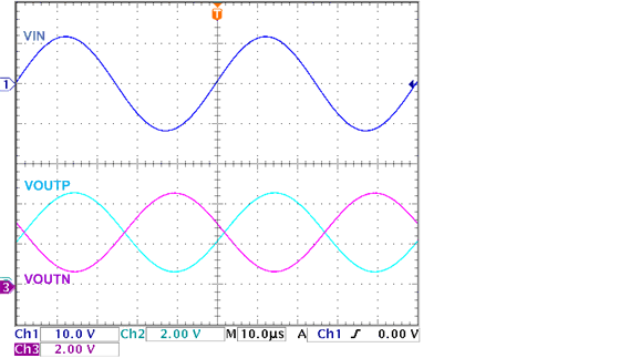
Figure 50 shows the typical AC response of the device with a full-scale sine wave with a frequency of 20 kHz applied at the input.
