JAJS331P July 2006 – August 2018 ISO7220A , ISO7220B , ISO7220C , ISO7220M , ISO7221A , ISO7221B , ISO7221C , ISO7221M
PRODUCTION DATA.
- 1 特長
- 2 アプリケーション
- 3 概要
- 4 改訂履歴
- 5 说明(续)
- 6 Pin Configuration and Functions
-
7 Specifications
- 7.1 Absolute Maximum Ratings
- 7.2 ESD Ratings
- 7.3 Recommended Operating Conditions
- 7.4 Thermal Information
- 7.5 Power Ratings
- 7.6 Insulation Specifications
- 7.7 Safety-Related Certifications
- 7.8 Safety Limiting Values
- 7.9 Electrical Characteristics—5-V VCC1 and V CC2 Supplies
- 7.10 Electrical Characteristics—5-V VCC1 and 3.3-V VCC2 Supply
- 7.11 Electrical Characteristics—3.3-V VCC1 and 5-V VCC2 Supply
- 7.12 Electrical Characteristics—3.3-V VCC1 and VCC2 Supplies
- 7.13 Electrical Characteristics—2.8-V VCC1 and VCC2 Supplies
- 7.14 Switching Characteristics—5-V VCC1 and VCC2 Supplies
- 7.15 Switching Characteristics—5-V VCC1 and 3.3-V VCC2 Supply
- 7.16 Switching Characteristics—3.3-V CC1 and 5-V VCC2 Supplies
- 7.17 Switching Characteristics—3.3-V VCC1 and VCC2 Supplies
- 7.18 Switching Characteristics—2.8-V VCC1 and VCC2 Supplies
- 7.19 Insulation Characteristics Curves
- 7.20 Typical Characteristics
- 8 Parameter Measurement Information
- 9 Detailed Description
- 10Application and Implementation
- 11Power Supply Recommendations
- 12Layout
- 13デバイスおよびドキュメントのサポート
- 14メカニカル、パッケージ、および注文情報
8 Parameter Measurement Information

A. The input pulse is supplied by a generator having the following characteristics: PRR ≤ 50 kHz, 50% duty cycle, tr ≤ 3 ns, tf ≤ 3 ns, ZO = 50 Ω.
B. CL = 15 pF and includes instrumentation and fixture capacitance within ± 20%.
Figure 14. Switching Characteristic Test Circuit and Voltage Waveforms 
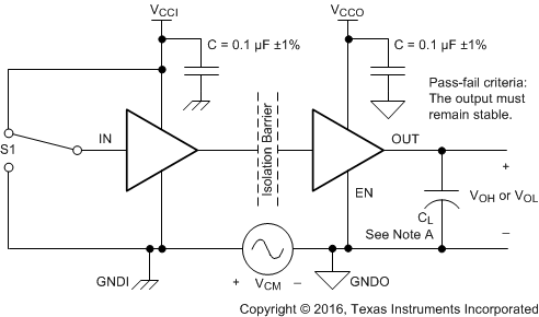
A. CL = 15 pF and includes instrumentation and fixture capacitance within ± 20%.
Figure 15. Failsafe Delay Time Test Circuit and Voltage Waveforms 
A. CL = 15 pF and includes instrumentation and fixture capacitance within ± 20%.
Figure 16. Common-Mode Transient Immunity Test Circuit 
NOTE:
PRBS bit pattern run length is 216 – 1. Transition time is 800 ps.