SNVS033D May 2004 – November 2015 LM2621
PRODUCTION DATA.
- 1 Features
- 2 Applications
- 3 Description
- 4 Revision History
- 5 Pin Configuration and Functions
- 6 Specifications
- 7 Detailed Description
-
8 Application and Implementation
- 8.1 Application Information
- 8.2 Typical Applications
- 9 Power Supply Recommendations
- 10Layout
- 11Device and Documentation Support
- 12Mechanical, Packaging, and Orderable Information
8 Application and Implementation
NOTE
Information in the following applications sections is not part of the TI component specification, and TI does not warrant its accuracy or completeness. TI’s customers are responsible for determining suitability of components for their purposes. Customers should validate and test their design implementation to confirm system functionality.
8.1 Application Information
The LM2621 is primarily used as a Boost type step-up converter. The following section provides information regarding connection and component choices to build a successful boost converter. Examples of typical applications are also provided including a SEPIC step-up/step-down topology. More details on designing a SEPIC converter can be found here: SLYT309.
8.2 Typical Applications
8.2.1 Step-Up DC-DC Converter Typical Application Using LM2621
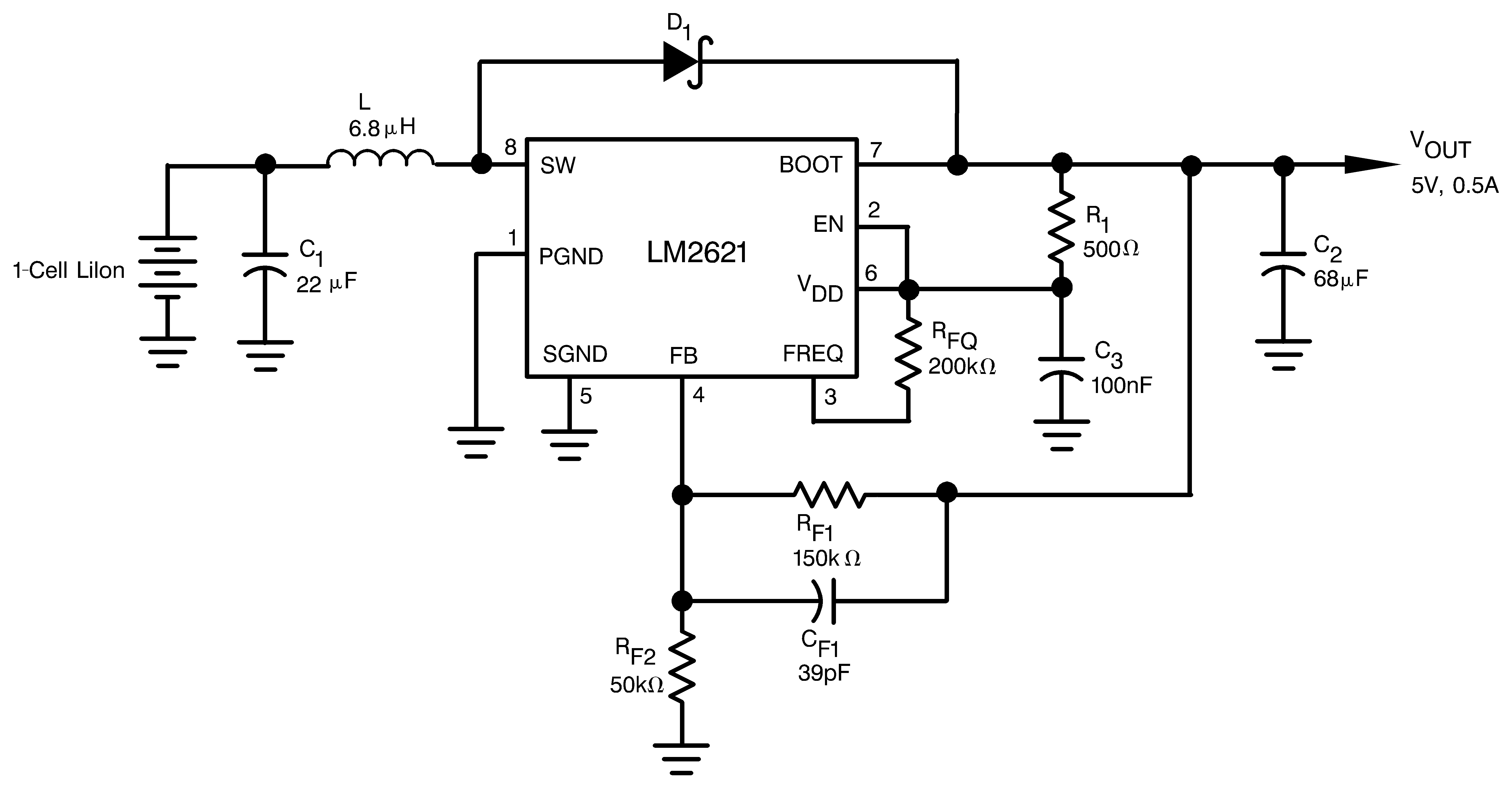 Figure 13. Typical Circuit
8.2.1.1 Design Requirements
In order to successfully build an application, the designer should have the following parameters:
- Output voltage to set the feedback voltage divider and to assess the source for biasing the VDD pin.
- Input voltage range (min and max) to ensure safe operation within absolute max. rating of the IC.
- Output current to ensure that the system will not hit the internal peak current limit of the IC (2.85 A typical) during normal operation.
8.2.1.2 Detailed Design Procedure
8.2.1.2.1 Setting the Output Voltage
The output voltage of the step-up regulator can be set between 1.24 V and 14 V by connecting a feedback resistive divider made of RF1 and RF2. The resistor values are selected as follows:
A value of 150 kΩ is suggested for RF1. Then, RF2 can be selected using the above equation. A 39-pF capacitor (CF1) connected across RF1 helps in feeding back most of the AC ripple at VOUT to the FB pin. This helps reduce the peak-to-peak output voltage ripple as well as improve the efficiency of the step-up regulator, because a set hysteresis of 30 mV at the FB pin is used for the gated oscillator control scheme.
8.2.1.2.2 Bootstrapping
When the output voltage (VOUT) is between 2.5 V and 5.0 V a bootstrapped operation is suggested. This is achieved by connecting the VDD pin (Pin 6) to VOUT. However if the VOUT is outside this range, the VDD pin should be connected to a voltage source whose range is between 2.5 V and 5 V. This can be the input voltage (VIN), VOUT stepped down using a linear regulator, or a different voltage source available in the system. This is referred to as non-bootstrapped operation. The maximum acceptable voltage at the BOOT pin (Pin 7) is 10 V.
8.2.1.2.3 Setting the Switching Frequency
The switching frequency of the oscillator is selected by choosing an external resistor (RFQ) connected between FREQ and VDD pins. See Figure 9 for choosing the RFQ value to achieve the desired switching frequency. A high switching frequency allows the use of very small surface mount inductors and capacitors and results in a very small solution size. A switching frequency between 300 kHz and 2 MHz is recommended.
8.2.1.2.4 Inductor Selection
The LM2621's high switching frequency enables the use of a small surface mount inductor. A 6.8-µH shielded inductor is suggested. The inductor should have a saturation current rating higher than the peak current it will experience during circuit operation (see Figure 10). Less than 100-mΩ ESR is suggested for high efficiency.
Open-core inductors cause flux linkage with circuit components and interfere with the normal operation of the circuit. They should be avoided. For high efficiency, choose an inductor with a high frequency core material, such as ferrite, to reduce the core losses. To minimize radiated noise, use a toroid, pot core or shielded core inductor. The inductor should be connected to the SW pin as close to the IC as possible. See Table 1 for a list of the inductor manufacturers.
8.2.1.2.5 Output Diode Selection
A Schottky diode should be used for the output diode. The forward current rating of the diode should be higher than the load current, and the reverse voltage rating must be higher than the output voltage. Do not use ordinary rectifier diodes, since slow switching speeds and long recovery times cause the efficiency and the load regulation to suffer. Table 1 shows a list of the diode manufacturers.
8.2.1.2.6 Input and Output Filter Capacitors Selection
Tantalum chip capacitors are recommended for the input and output filter capacitors. A 22-µF capacitor is suggested for the input filter capacitor. It should have a DC working voltage rating higher than the maximum input voltage. A 68-µF tantalum capacitor is suggested for the output capacitor. The DC working voltage rating should be greater than the output voltage. Very high ESR values (> 3Ω) should be avoided.
8.2.1.3 Application Curves
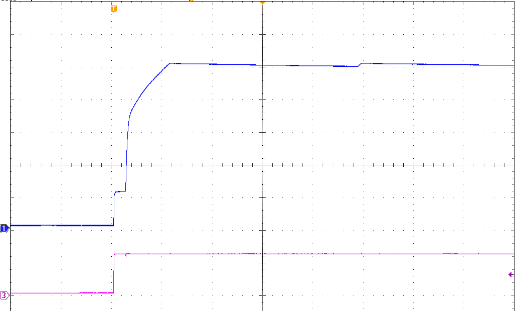 Figure 14. Startup Vin=1.2V,Vout-5V, 10ms/div 1V/div (Ch3:Vin,Ch1:Vout)
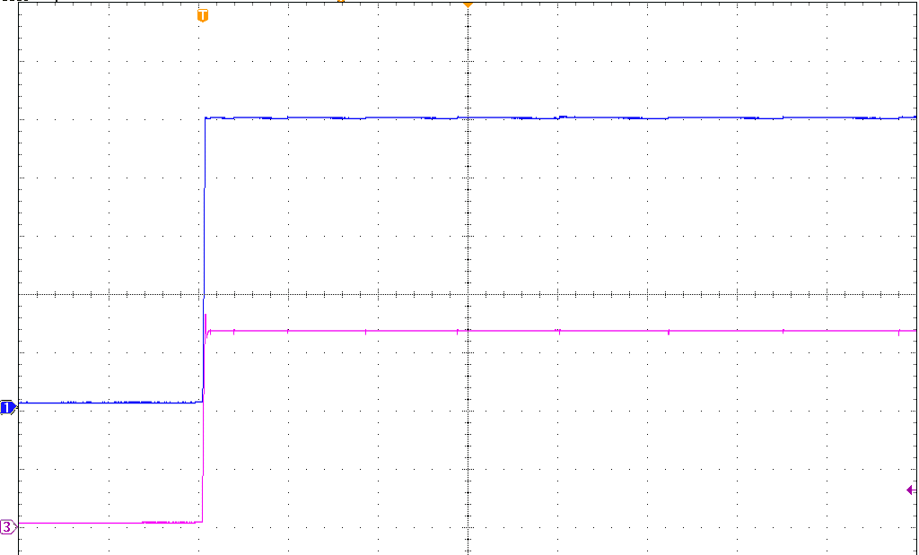 Figure 15. Startup Vin=3.3V,Vout-5V, 10ms/div 1V/div (Ch3:Vin,Ch1:Vout)
8.2.2 5-V / 0.5-A Step-Up Regulator
 Figure 16. 5-V/0.5A Step-Up Regulator
8.2.2.1 Design Requirements
Design requirement is the same to the typical application shown earlier. Components have been chosen that comply with the required maximum height. See Design Requirements for the design requirement and following sections for the detailed design procedure.
8.2.2.2 Detailed Design Procedure
Follow the detailed design procedure in Detailed Design Procedure.
Table 1. Bill of Materials
| Manufacturer | Part Number | |
|---|---|---|
| U1 | TI | LM2621MM |
| C1 | Vishay/Sprague | 595D226X06R3B2T, Tantalum |
| C2 | Vishay/Sprague | 595D686X0010C2T, Tantalum |
| D1 | Motorola | MBRS140T3 |
| L | Coilcraft | DT1608C-682 |
8.2.3 2-mm Tall 5-V / 0.2-A Step-Up Regulator for Low Profile Applications
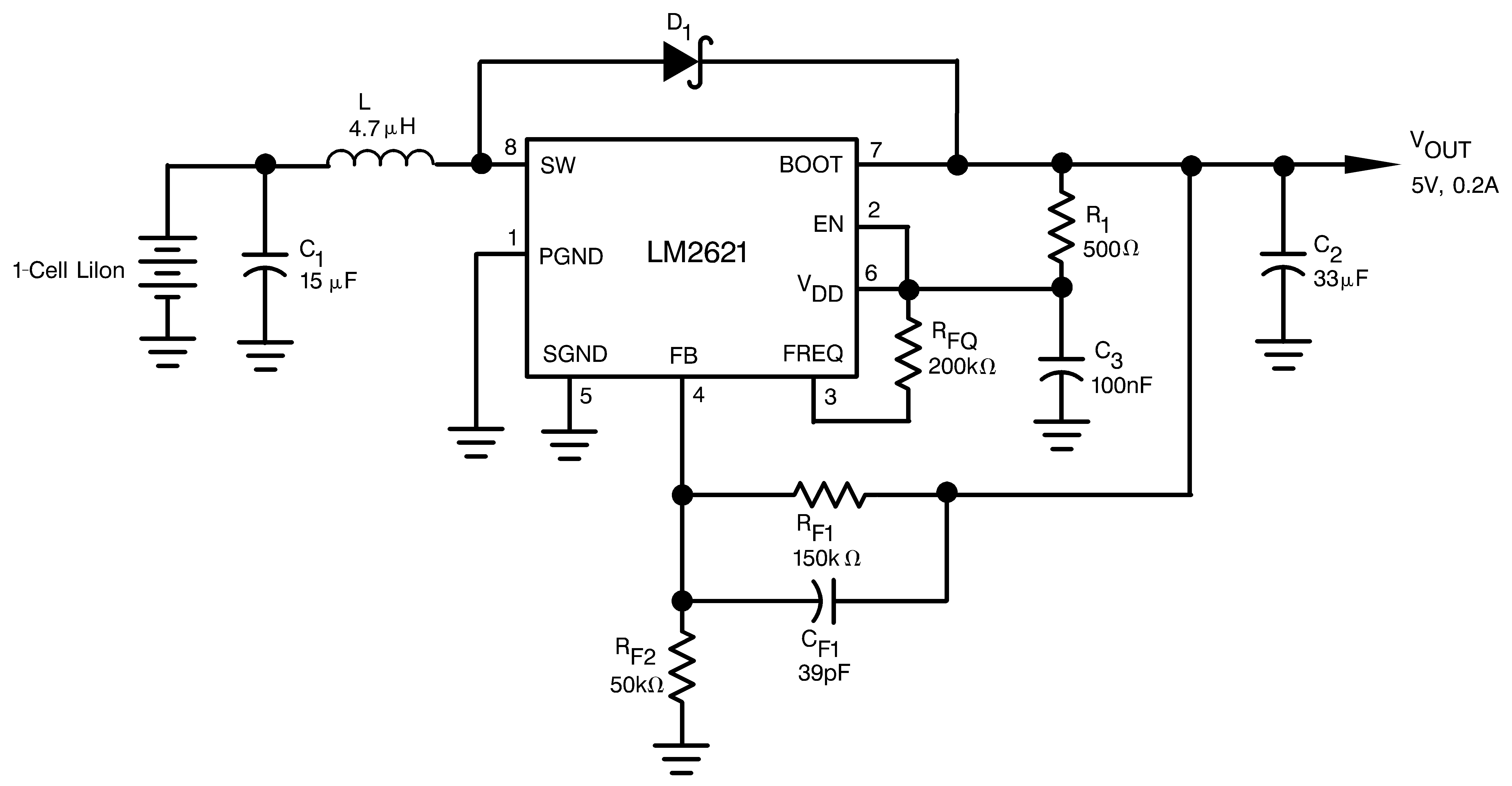 Figure 17. 2-mm Tall 5-V/0.2A Step-Up Regulator for Low Profile Applications
8.2.3.1 Design Requirements
Design requirement is the same to the typical application shown earlier. Components have been chosen that comply with the required maximum height. See Design Requirements for the design requirement and following sections for the detailed design procedure.
8.2.3.2 Detailed Design Procedure
Follow the detailed design procedure in Detailed Design Procedure.
Table 2. Bill of Materials
| Manufacturer | Part Number | |
|---|---|---|
| U1 | TI | LM2621MM |
| C1 | Vishay/Sprague | 592D156X06R3B2T, Tantalum |
| C2 | Vishay/Sprague | 592D336X06R3C2T, Tantalum |
| D1 | Motorola | MBRS140T3 |
| L | Vishay/Dale | ILS-3825-03 |
8.2.4 3.3-V / 0.5-A SEPIC Regulator
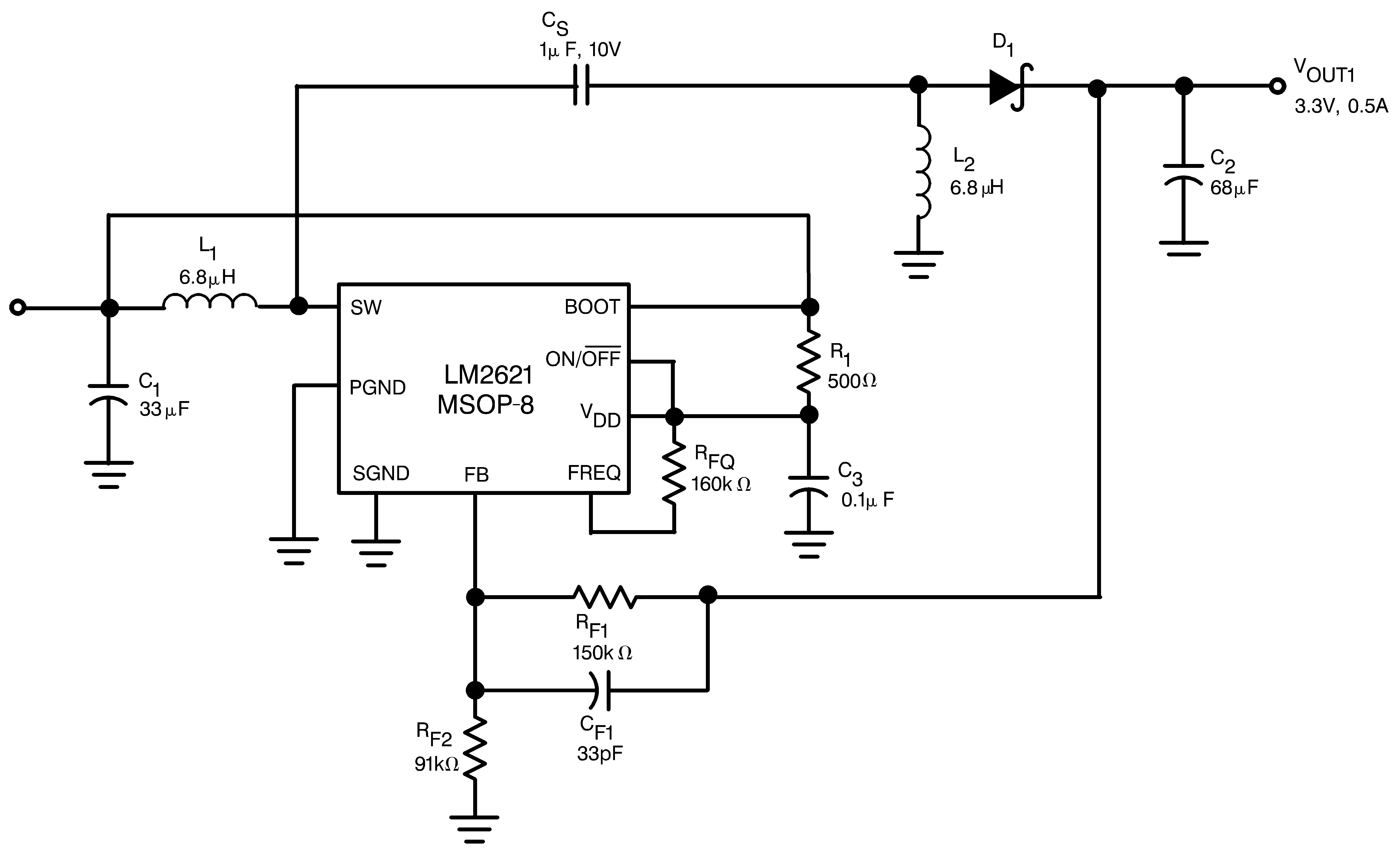 Figure 18. 3.3-V/0.5-A SEPIC Regulator
8.2.4.1 Design Requirements
Design requirement for the SEPIC is similar to that of a boost but the current flowing through the switch is the addition of the current flowing through L1 and L2. As a result, the peak current through the main switch is IIN+IOUT+0.5xDeltaIL1+0.5xDeltaIL2. See SLYT309 for detail on the specific design requirement of a SEPIC converter.
8.2.4.2 Detailed Design Procedure
Follow the detailed design procedure in Detailed Design Procedure.
Table 3. Bill of Materials
| Manufacturer | Part Number | Description | |
|---|---|---|---|
| U1 | TI | LM2621MM | Low Input Voltage Regulator |
| C1 | Sanyo | 10CV220AX, SMT AL-Electrolytic | 220 µF |
| C2 | TDK | C2012X7R1C225M, MLCC | 2.2 µF |
| C3 | Vishay | VJ0603A331KXXAT | 33 pF |
| C4 | TDK | C3225X7R0J107MT | 100 µF |
| C5, C6 | Vishay | VJ0603Y104KXXAT | 0.1 µF |
| D1 | Philips | BAT54C | VR = 1V |
| D2 | Vishay | MBRS120 | 1A / VR = 20V |
| L1, L2 | Coilcraft | DO1813P-682HC | 6.8 µH |
| R1 | Vishay | CRCW08054990FRT6 | 499 Ω |
| R2 | Vishay | CRCW08051503FRT6 | 150 kΩ |
| R3 | Vishay | CRCW08053923FRT6 | 392 kΩ |
| R4 | Vishay | CRCW08059092FRT6 | 90.9 kΩ |