SNVS033D May 2004 – November 2015 LM2621
PRODUCTION DATA.
- 1 Features
- 2 Applications
- 3 Description
- 4 Revision History
- 5 Pin Configuration and Functions
- 6 Specifications
- 7 Detailed Description
-
8 Application and Implementation
- 8.1 Application Information
- 8.2 Typical Applications
- 9 Power Supply Recommendations
- 10Layout
- 11Device and Documentation Support
- 12Mechanical, Packaging, and Orderable Information
7 Detailed Description
7.1 Overview
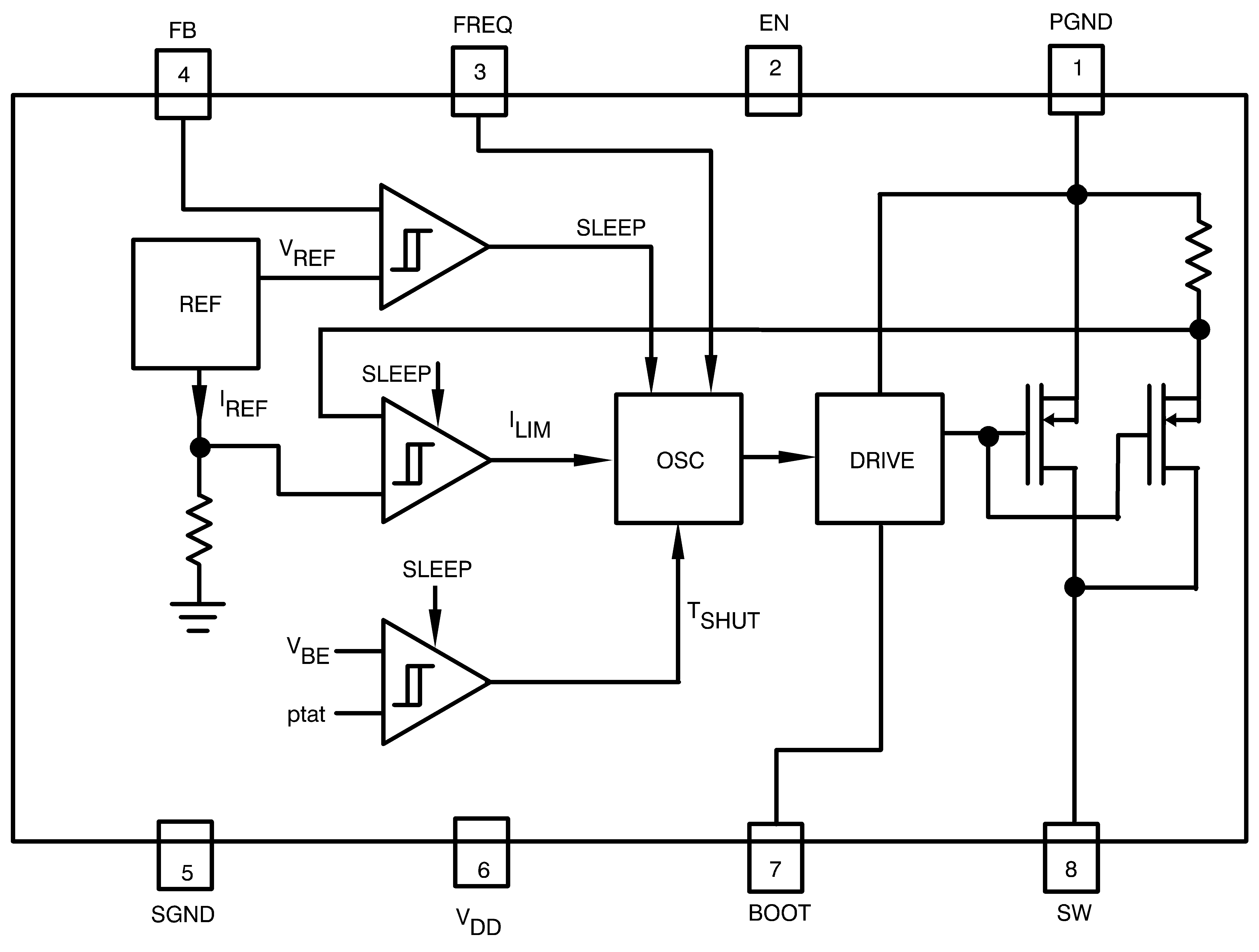
The LM2621 is designed to provide step-up DC-DC voltage regulation in battery-powered and low-input voltage systems. It combines a step-up switching regulator, N-channel power MOSFET, built-in current limit, thermal limit, and voltage reference in a single 8-pin VSSOP package Pin Configuration and Functions. The switching DC-DC regulator boosts an input voltage between 1.2 V and 14 V to a regulated output voltage between 1.24 V and 14 V. The LM2621 starts from a low 1.1-V input and remains operational down to 0.65 V.
This device is optimized for use in cellular phones and other applications requiring a small size, low profile, as well as low quiescent current for maximum battery life during stand-by and shutdown. A high-efficiency gated-oscillator topology offers an output of up to 1 A.
Additional features include a built-in peak switch current limit, and thermal protection circuitry.
7.2 Functional Block Diagram

7.3 Feature Description
7.3.1 Gated Oscillator Control Scheme
A unique gated oscillator control scheme enables the LM2621 to have an ultra-low quiescent current and provides a high efficiency over a wide load range. The switching frequency of the internal oscillator is programmable using an external resistor and can be set between 300 kHz and 2 MHz.
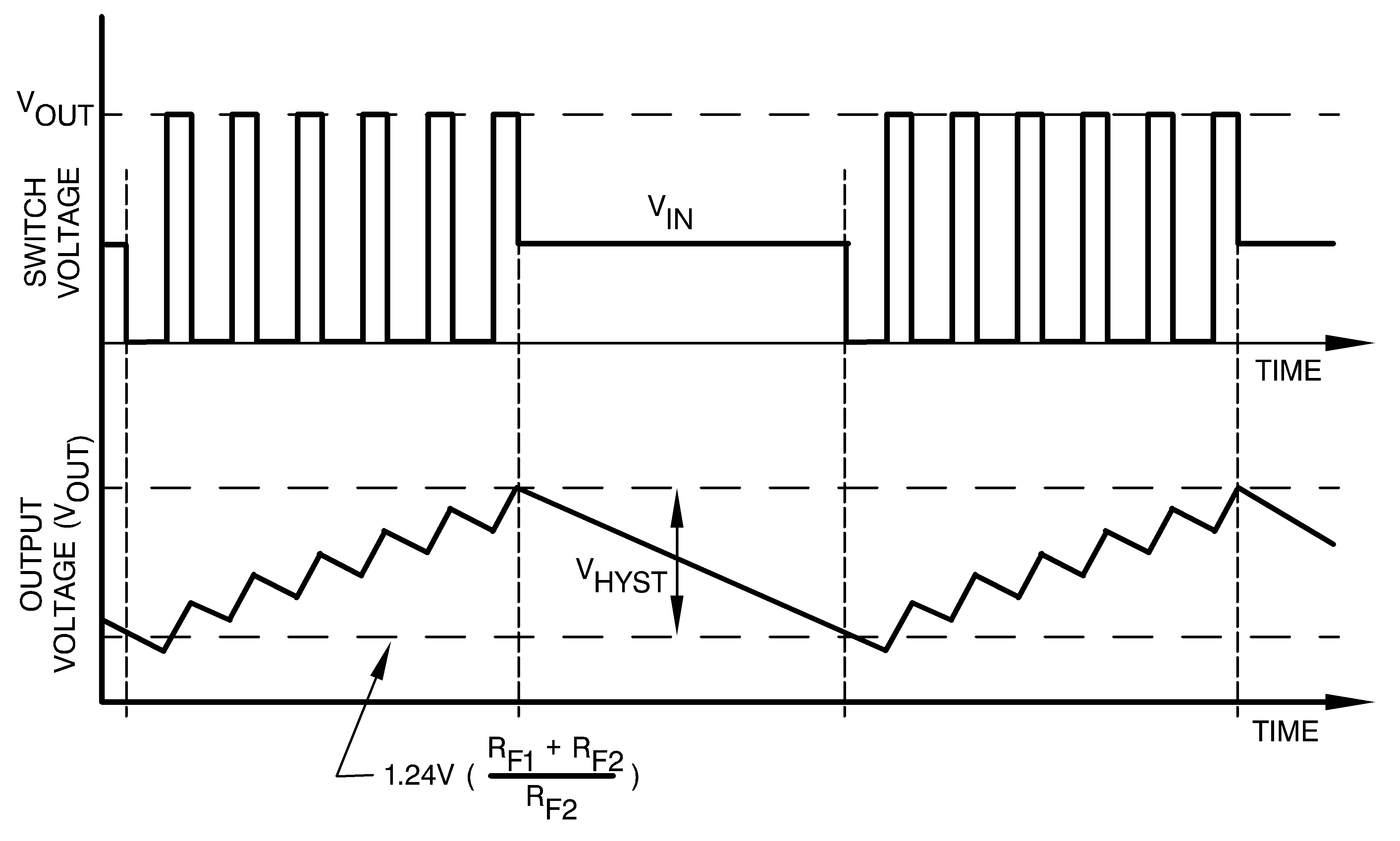
This control scheme uses a hysteresis window to regulate the output voltage. When the output voltage is below the upper threshold of the window, the LM2621 switches continuously with a fixed duty cycle of 70% at the switching frequency selected by the user. During the first part of each switching cycle, the internal N-channel MOSFET switch is turned on. This causes the current to ramp up in the inductor and store energy. During the second part of each switching cycle, the MOSFET is turned off. The voltage across the inductor reverses and forces current through the diode to the output filter capacitor and the load. Thus when the LM2621 switches continuously, the output voltage starts to ramp up. When the output voltage hits the upper threshold of the window, the LM2621 stops switching completely. This causes the output voltage to droop because the energy stored in the output capacitor is depleted by the load. When the output voltage hits the lower threshold of the hysteresis window, the LM2621 starts switching continuously again causing the output voltage to ramp up towards the upper threshold. Figure 12 shows the switch voltage and output voltage waveforms.
Because of this type of control scheme, the quiescent current is inherently very low. At light loads the gated oscillator control scheme offers a much higher efficiency compared to the conventional PWM control scheme.
 Figure 12. Typical Step-Up Regulator Waveforms
7.3.2 Low Voltage Start-Up
The LM2621 can start-up from input voltages as low as 1.1 V. On start-up, the control circuitry switches the N-channel MOSFET continuously at 70% duty cycle until the output voltage reaches 2.5 V. After this output voltage is reached, the normal step-up regulator feedback and gated oscillator control scheme take over. Once the device is in regulation it can operate down to a 0.65-V input, since the internal power for the IC can be boot-strapped from the output using the VDD pin.
7.3.3 Output Voltage Ripple Frequency
A major component of the output voltage ripple is due to the hysteresis used in the gated oscillator control scheme. The frequency of this voltage ripple is proportional to the load current. The frequency of this ripple does not necessitate the use of larger inductors and capacitors however, since the size of these components is determined by the switching frequency of the oscillator which can be set up to 2 MHz using an external resistor.
7.3.4 Internal Current Limit and Thermal Protection
An internal cycle-by-cycle current limit serves as a protection feature. This is set high enough (2.85 A typical, approximately 4 A maximum) so as not to come into effect during normal operating conditions. An internal thermal protection circuitry disables the MOSFET power switch when the junction temperature (TJ) exceeds about 160°C. The switch is re-enabled when TJ drops below approximately 135°C.
7.4 Device Functional Modes
7.4.1 Shutdown
The LM2621 features a shutdown mode that reduces the quiescent current to less than a specified 2.5-µA overtemperature. This extends the life of the battery in battery powered applications. During shutdown, all feedback and control circuitry is turned off. The regulator's output voltage drops to one diode drop below the input voltage. Entry into the shutdown mode is controlled by the active-low logic input pin EN (Pin 2). When the logic input to this pin pulled below 0.15 VDD, the device goes into shutdown mode. The logic input to this pin should be above 0.7 VDD for the device to work in normal step-up mode.