SNVS033D May   2004  – November 2015 LM2621

PRODUCTION DATA.  

  1. Features
  2. Applications
  3. Description
  4. Revision History
  5. Pin Configuration and Functions
  6. Specifications
    1. 6.1 Absolute Maximum Ratings
    2. 6.2 Recommended Operating Conditions
    3. 6.3 Thermal Information
    4. 6.4 Electrical Characteristics
    5. 6.5 Typical Characteristics
  7. Detailed Description
    1. 7.1 Overview
    2. 7.2 Functional Block Diagram
    3. 7.3 Feature Description
      1. 7.3.1 Gated Oscillator Control Scheme
      2. 7.3.2 Low Voltage Start-Up
      3. 7.3.3 Output Voltage Ripple Frequency
      4. 7.3.4 Internal Current Limit and Thermal Protection
    4. 7.4 Device Functional Modes
      1. 7.4.1 Shutdown
  8. Application and Implementation
    1. 8.1 Application Information
    2. 8.2 Typical Applications
      1. 8.2.1 Step-Up DC-DC Converter Typical Application Using LM2621
        1. 8.2.1.1 Design Requirements
        2. 8.2.1.2 Detailed Design Procedure
          1. 8.2.1.2.1 Setting the Output Voltage
          2. 8.2.1.2.2 Bootstrapping
          3. 8.2.1.2.3 Setting the Switching Frequency
          4. 8.2.1.2.4 Inductor Selection
          5. 8.2.1.2.5 Output Diode Selection
          6. 8.2.1.2.6 Input and Output Filter Capacitors Selection
        3. 8.2.1.3 Application Curves
      2. 8.2.2 5-V / 0.5-A Step-Up Regulator
        1. 8.2.2.1 Design Requirements
        2. 8.2.2.2 Detailed Design Procedure
      3. 8.2.3 2-mm Tall 5-V / 0.2-A Step-Up Regulator for Low Profile Applications
        1. 8.2.3.1 Design Requirements
        2. 8.2.3.2 Detailed Design Procedure
      4. 8.2.4 3.3-V / 0.5-A SEPIC Regulator
        1. 8.2.4.1 Design Requirements
        2. 8.2.4.2 Detailed Design Procedure
  9. Power Supply Recommendations
  10. 10Layout
    1. 10.1 Layout Guidelines
    2. 10.2 Layout Example
  11. 11Device and Documentation Support
    1. 11.1 Device Support
      1. 11.1.1 Third-Party Products Disclaimer
    2. 11.2 Documentation Support
      1. 11.2.1 Related Documentation
    3. 11.3 Community Resources
    4. 11.4 Trademarks
    5. 11.5 Electrostatic Discharge Caution
    6. 11.6 Glossary
  12. 12Mechanical, Packaging, and Orderable Information

パッケージ・オプション

メカニカル・データ(パッケージ|ピン)
サーマルパッド・メカニカル・データ

10 Layout

10.1 Layout Guidelines

High switching frequencies and high peak currents make a proper layout of the PC board an important part of design. Poor design can cause excessive EMI and ground-bounce, both of which can cause malfunction and loss of regulation by corrupting voltage feedback signal and injecting noise into the control section.

Power components - such as the inductor, input and output filter capacitors, and output diode - should be placed as close to the regulator IC as possible, and their traces should be kept short, direct and wide. The ground pins of the input and output filter capacitors and the PGND and SGND pins of LM2621 should be connected using short, direct and wide traces. The voltage feedback network (RF1, RF2, and CF1) should be kept very close to the FB pin. Noisy traces, such as from the SW pin, should be kept away from the FB and VDD pins. The traces that run between Vout and the FB pin of the IC should be kept away from the inductor flux. Always provide sufficient copper area to dissipate the heat due to power loss in the circuitry and prevent the thermal protection circuitry in the IC from shutting the IC down.

10.2 Layout Example
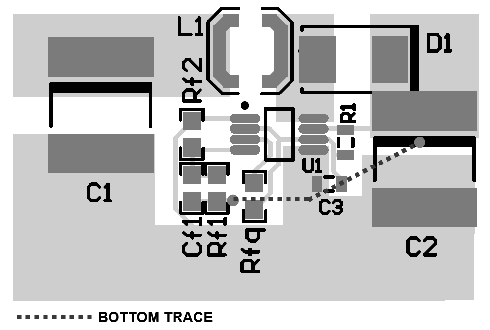
LM2621 typical_layout_snvs033.png Figure 19. LM2621 PCB Layout