SNVS188I May 2004 – October 2017 LM2623
PRODUCTION DATA.
- 1 Features
- 2 Applications
- 3 Description
- 4 Revision History
- 5 Pin Configuration And Functions
- 6 Specifications
- 7 Detailed Description
- 8 Applications And Implementation
- 9 Power Supply Recommendations
- 10Layout
- 11Device And Documentation Support
- 12Mechanical, Packaging, And Orderable Information
パッケージ・オプション
メカニカル・データ(パッケージ|ピン)
サーマルパッド・メカニカル・データ
発注情報
7 Detailed Description
7.1 Overview
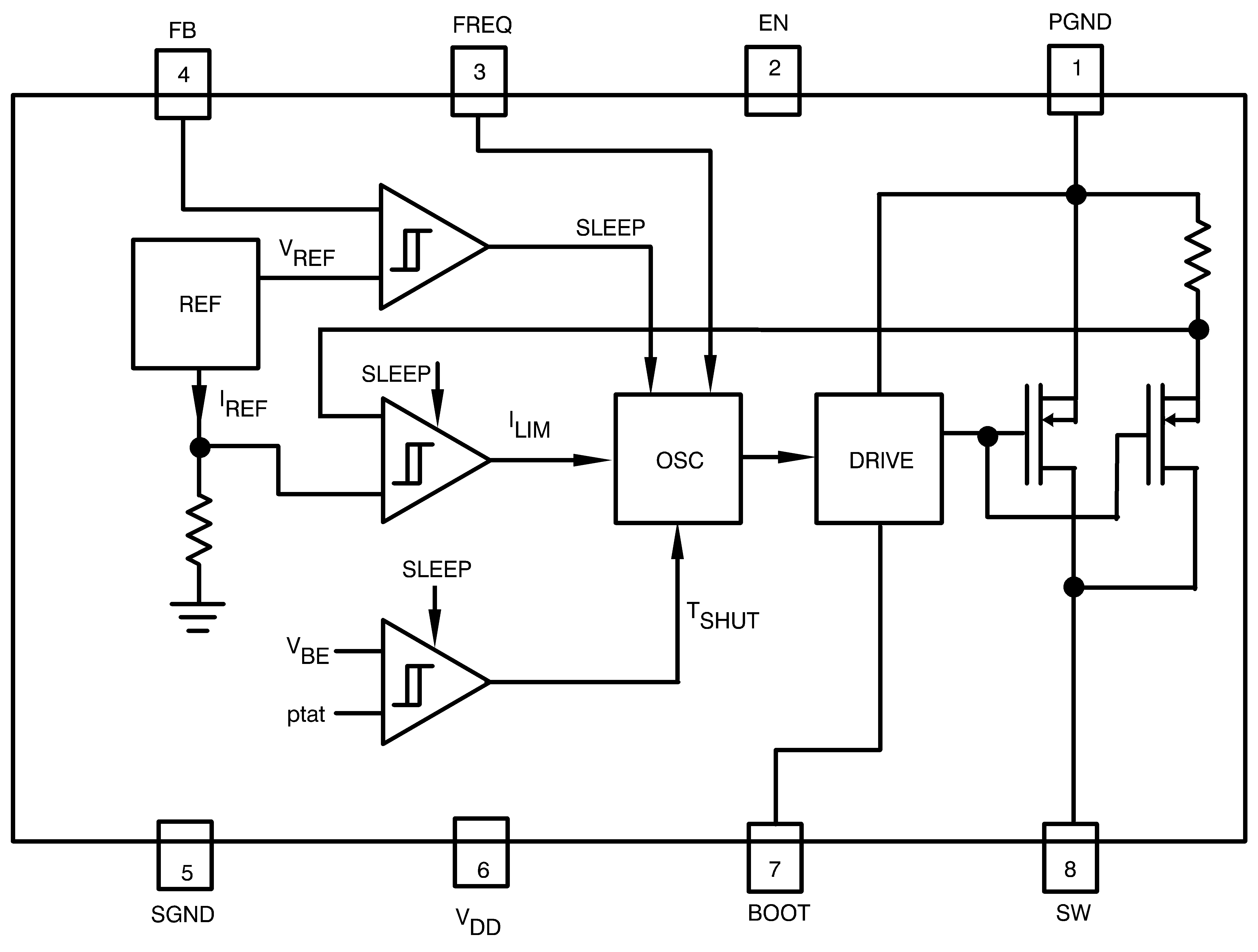
The LM2623 is designed to provide step-up DC-DC voltage regulation in battery-powered and low-input voltage systems. It combines a step-up switching regulator, N-channel power MOSFET, built-in current limit, thermal limit, and voltage reference in a single 8-pin VSSOP package Functional Block Diagram. The switching DC-DC regulator boosts an input voltage between 0.8 V and 14 V to a regulated output voltage between 1.24 V and 14 V. The LM2623 starts from a low 1.1 V input and remains operational down to below 0.8 V.
This device is optimized for use in cellular phones and other applications requiring a small size, low profile, as well as low quiescent current for maximum battery life during stand-by and shutdown. A high-efficiency gated-oscillator topology offers an output of up to 2 A at low output voltages.
Additional features include a built-in peak switch current limit, and thermal protection circuitry.
7.2 Functional Block Diagram

7.3 Feature Description
7.3.1 Gated Oscillator Control Scheme.
The on/off regulation mode of the LM2623, along with its ultra-low quiescent current, results in good efficiency over a very wide load range. The internal oscillator frequency can be programmed using an external resistor to be constant or vary with the battery voltage. Adding a capacitor to program the frequency allows the designer to adjust the duty cycle and optimize it for the application. Adding a resistor in addition to the capacitor allows the duty cycle to dynamically compensate for changes to the input/output voltage ratio. We call this a Ratio Adaptive Gated Oscillator circuit. See the Typical Application for sample application circuits. Using the correct RC components to adjust the oscillator allows the part to run with low ripple and high efficiency over a wide range of loads and input/output voltages.
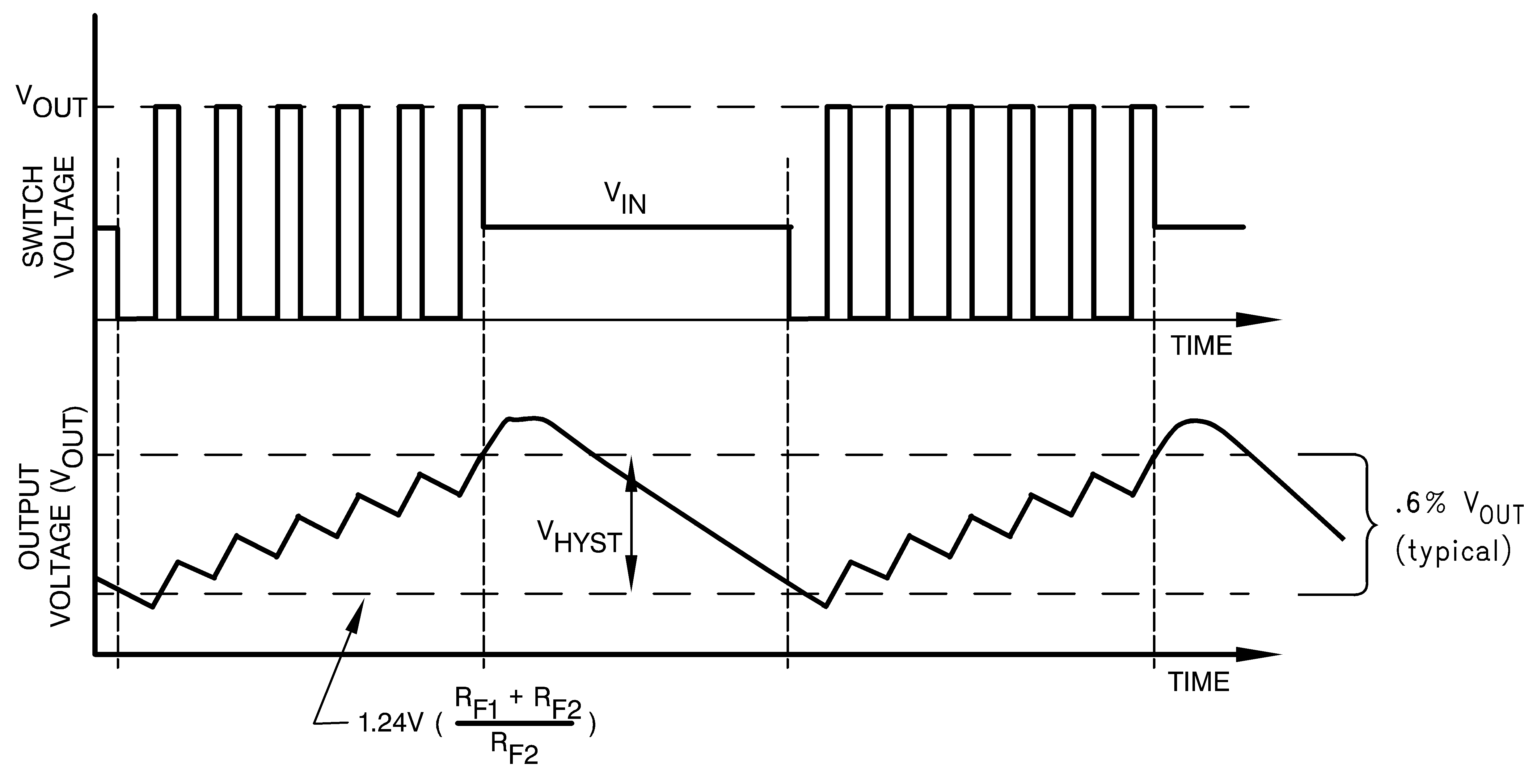
 Figure 8. Typical Step-Up Regulator Waveforms
7.3.2 Cycle-To-Cycle Pfm
When the load doesn't vary over a wide range (like zero to full load), ratio adaptive circuit techniques can be used to achieve cycle to cycle PFM regulation and lower ripple (or smaller output capacitors). The key to success here is matching the duty cycle of the circuit closely to what is required by the input to output voltage ratio. This ratio then needs to be dynamically adjusted for input voltage changes (usually caused by batteries running down). The chosen ratio should allow most of the energy in each switching cycle to be delivered to the load and only a small amount to be stored. When the regulation limit is reached, the overshoot will be small and the system will settle at an equilibrium point where it adjusts the off time in each switching cycle to meet the current requirements of the load. The off time adjustment is done by exceeding the regulation limit during each switching cycle and waiting until the voltage drops below the limit again to start the next switching cycle. The current in the coil never goes to zero like it frequently does in the hysteretic operating mode of circuits with wide load variations or duty cycles that aren't matched to the input/output voltage ratio. Optimizing the duty cycle for a given set of input/output voltages conditions can be done by using the circuit values in the Application Notes.
7.3.3 Shutdown
The LM2623 features a shutdown mode that reduces the quiescent current to less than an ensured 2.5 µA over temperature. This extends the life of the battery in battery powered applications. During shutdown, all feedback and control circuitry is turned off. The regulator's output voltage drops to one diode drop below the input voltage. Entry into the shutdown mode is controlled by the active-low logic input pin EN (pin-2). When the logic input to this pin is pulled below 0.15 VDD, the device goes into shutdown mode. The logic input to this pin should be above 0.7 VDD for the device to work in normal stepup mode.
7.3.4 Internal Current Limit And Thermal Protection
An internal cycle-by-cycle current limit serves as a protection feature. This is set high enough (2.85 A typical, approximately 4 A maximum) so as not to come into effect during normal operating conditions. An internal thermal protection circuit disables the MOSFET power switch when the junction temperature (TJ) exceeds about 160°C. The switch is re-enabled when TJ drops below approximately 135°C.
7.4 Device Functional Modes
7.4.1 Pulse Frequency Modulation (Pfm)
Pulse Frequency Modulation is typically accomplished by switching continuously until the voltage limit is reached and skipping cycles after that to just maintain it. This results in a somewhat hysteretic mode of operation. The coil stores more energy each cycle as the current ramps up to high levels. When the voltage limit is reached, the system usually overshoots to a higher voltage than required, due to the stored energy in the coil (see Figure 8). The system will also undershoot somewhat when it starts switching again because it has depleted all the stored energy in the coil and needs to store more energy to reach equilibrium with the load. Larger output capacitors and smaller inductors reduce the ripple in these situations. The frequency being filtered, however, is not the basic switching frequency. It is a lower frequency determined by the load, the input/output voltage and the circuit parameters. This mode of operation is useful in situations where the load variation is significant. Power managed computer systems, for instance, may vary from zero to full load while the system is on and this is usually the preferred regulation mode for such systems.
7.4.2 Low Voltage Start-Up
The LM2623 can start up from voltages as low as 1.1 V. On start-up, the control circuitry switches the N-channel MOSFET continuously until the output reaches 3 V. After this output voltage is reached, the normal step-up regulator feedback and gated oscillator control scheme take over. Once the device is in regulation, it can operate down to below 0.8 V input, since the internal power for the IC can be boot-strapped from the output using the VDD pin.