JAJSAY9L February   2009  – May 2018 LM26420

PRODUCTION DATA.  

  1. 特長
  2. アプリケーション
  3. 概要
    1.     Device Images
      1.      LM26420デュアル降圧DC/DCコンバータ
      2.      LM26420の効率(最高93%)
  4. 改訂履歴
  5. Pin Configuration and Functions
    1.     Pin Functions: 16-Pin WQFN
    2.     Pin Functions 20-Pin HTSSOP
  6. Specifications
    1. 6.1 Absolute Maximum Ratings
    2. 6.2 ESD Ratings (LM26420X/Y)
    3. 6.3 Recommended Operating Conditions
    4. 6.4 Thermal Information
    5. 6.5 Electrical Characteristics Per Buck
    6. 6.6 Typical Characteristics
  7. Detailed Description
    1. 7.1 Overview
    2. 7.2 Functional Block Diagram
    3. 7.3 Feature Description
      1. 7.3.1 Soft Start
      2. 7.3.2 Power Good
      3. 7.3.3 Precision Enable
    4. 7.4 Device Functional Modes
      1. 7.4.1 Output Overvoltage Protection
      2. 7.4.2 Undervoltage Lockout
      3. 7.4.3 Current Limit
      4. 7.4.4 Thermal Shutdown
  8. Application and Implementation
    1. 8.1 Application Information
      1. 8.1.1 Programming Output Voltage
      2. 8.1.2 VINC Filtering Components
      3. 8.1.3 Using Precision Enable and Power Good
      4. 8.1.4 Overcurrent Protection
    2. 8.2 Typical Applications
      1. 8.2.1 LM26420X 2.2-MHz, 0.8-V Typical High-Efficiency Application Circuit
        1. 8.2.1.1 Design Requirements
        2. 8.2.1.2 Detailed Design Procedure
          1. 8.2.1.2.1 Custom Design With WEBENCH® Tools
          2. 8.2.1.2.2 Inductor Selection
          3. 8.2.1.2.3 Input Capacitor Selection
          4. 8.2.1.2.4 Output Capacitor
          5. 8.2.1.2.5 Calculating Efficiency and Junction Temperature
        3. 8.2.1.3 Application Curves
      2. 8.2.2 LM26420X 2.2-MHz, 1.8-V Typical High-Efficiency Application Circuit
        1. 8.2.2.1 Design Requirements
        2. 8.2.2.2 Detailed Design Procedure
        3. 8.2.2.3 Application Curves
      3. 8.2.3 LM26420X 2.2-MHz, 2.5-V Typical High-Efficiency Application Circuit
        1. 8.2.3.1 Design Requirements
        2. 8.2.3.2 Detailed Design Procedure
        3. 8.2.3.3 Application Curves
      4. 8.2.4 LM26420Y 550 kHz, 0.8-V Typical High-Efficiency Application Circuit
        1. 8.2.4.1 Design Requirements
        2. 8.2.4.2 Detailed Design Procedure
        3. 8.2.4.3 Application Curves
      5. 8.2.5 LM26420Y 550-kHz, 1.8-V Typical High-Efficiency Application Circuit
        1. 8.2.5.1 Design Requirements
        2. 8.2.5.2 Detailed Design Procedure
        3. 8.2.5.3 Application Curves
      6. 8.2.6 LM26420Y 550-kHz, 2.5-V Typical High-Efficiency Application Circuit
        1. 8.2.6.1 Design Requirements
        2. 8.2.6.2 Detailed Design Procedure
        3. 8.2.6.3 Application Curves
  9. Power Supply Recommendations
  10. 10Layout
    1. 10.1 Layout Guidelines
    2. 10.2 Layout Example
    3. 10.3 Thermal Considerations
      1. 10.3.1 Method 1: Silicon Junction Temperature Determination
      2. 10.3.2 Thermal Shutdown Temperature Determination
  11. 11デバイスおよびドキュメントのサポート
    1. 11.1 デバイス・サポート
      1. 11.1.1 デベロッパー・ネットワークの製品に関する免責事項
      2. 11.1.2 WEBENCH®ツールによるカスタム設計
    2. 11.2 ドキュメントのサポート
      1. 11.2.1 関連資料
    3. 11.3 ドキュメントの更新通知を受け取る方法
    4. 11.4 コミュニティ・リソース
    5. 11.5 商標
    6. 11.6 静電気放電に関する注意事項
    7. 11.7 Glossary
  12. 12メカニカル、パッケージ、および注文情報

パッケージ・オプション

メカニカル・データ(パッケージ|ピン)
サーマルパッド・メカニカル・データ
発注情報

VINC Filtering Components

Additional filtering is required between VINC and AGND in order to prevent high frequency noise on VIN from disturbing the sensitive circuitry connected to VINC. A small RC filter can be used on the VINC pin as shown in Figure 30.
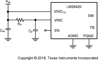
LM26420 30069638.gifFigure 30. RC Filter On VINC

In general, RF is typically between 1 Ω and 10 Ω so that the steady state voltage drop across the resistor due to the VINC bias current does not affect the UVLO level. CF can range from 0.22 µF to 1 µF in X7R or X5R dielectric, where the RC time constant should be at least 2 µs. CF must be placed as close to the device as possiblewith a direct connection from VINC and AGND.