JAJSAP6I June 2007 – September 2018 LM2735
PRODUCTION DATA.
- 1 特長
- 2 アプリケーション
- 3 概要
- 4 改訂履歴
- 5 Pin Configuration and Functions
- 6 Specifications
- 7 Detailed Description
-
8 Application and Implementation
- 8.1 Application Information
- 8.2
Typical Applications
- 8.2.1 LM2735X SOT-23 Design Example 1
- 8.2.2 LM2735Y SOT-23 Design Example 2
- 8.2.3 LM2735X WSON Design Example 3
- 8.2.4 LM2735Y WSON Design Example 4
- 8.2.5 LM2735Y MSOP-PowerPAD Design Example 5
- 8.2.6 LM2735X SOT-23 Design Example 6
- 8.2.7 LM2735Y SOT-23 Design Example 7
- 8.2.8 LM2735X SOT-23 Design Example 8
- 8.2.9 LM2735Y SOT-23 Design Example 9
- 8.2.10 LM2735X WSON Design Example 10
- 8.2.11 LM2735Y WSON Design Example 11
- 8.2.12 LM2735X WSON SEPIC Design Example 12
- 8.2.13 LM2735Y MSOP-PowerPAD SEPIC Design Example 13
- 8.2.14 LM2735X SOT-23 LED Design Example 14
- 8.2.15 LM2735Y WSON FlyBack Design Example 15
- 8.2.16 LM2735X SOT-23 LED Design Example 16 VRAIL > 5.5 V Application
- 8.2.17 LM2735X SOT-23 LED Design Example 17 Two-Input Voltage Rail Application
- 8.2.18 SEPIC Converter
- 9 Power Supply Recommendations
- 10Layout
- 11デバイスおよびドキュメントのサポート
- 12メカニカル、パッケージ、および注文情報
パッケージ・オプション
メカニカル・データ(パッケージ|ピン)
サーマルパッド・メカニカル・データ
- DGN|8
発注情報
10.3.5.2 Example From Previous Calculations
PDissipation = 475 mW
TA at Shutdown = 139°C
TCase-Top at Shutdown = 155°C

RθJA WSON = 55°C/W
RψJC WSON = 21°C/W
WSON & MSOP-PowerPAD typical applications will produce RθJA numbers in the range of 50°C/W to 65°C/W, and RψJC will vary from 18°C/W to 28°C/W. These values are for PCB’s with two and four layer boards with 0.5-oz copper, and 4 to 6 thermal vias to bottom side ground plane under the DAP.
For 5-pin SOT-23 package typical applications, RθJA numbers will range from 80°C/W to 110°C/W, and RψJC will vary from 50°C/W to 65°C/W. These values are for PCBs with 2- and 4-layer boards with 0.5-oz copper, with 2 to 4 thermal vias from GND pin to bottom layer.
The following is a good rule of thumb for typical thermal impedances, and an ambient temperature maximum of 75°C: if the design requires more than 400 mW internal to the LM2735 be dissipated, or there is 750 mW of total power loss in the application, TI recommends using the 6-pin WSON or the 8-pin MSOP-PowerPAD package.
NOTE
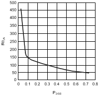
To use these procedures, it is important to dissipate an amount of power within the device that will indicate a true thermal impedance value. If a very small internal dissipated value is used, it can be determined that the thermal impedance calculated is abnormally high, and subject to error. The graph below shows the nonlinear relationship of internal power dissipation vs RθJA.
 Figure 50. RθJA vs Internal Dissipation for the WSON
and MSOP-PowerPAD Package