SNVSA85C October 2015 – January 2017 LM27761
PRODUCTION DATA.
- 1 Features
- 2 Applications
- 3 Description
- 4 Revision History
- 5 Pin Configuration and Functions
- 6 Specifications
- 7 Detailed Description
-
8 Application and Implementation
- 8.1 Application Information
- 8.2
Typical Application - Regulated Voltage Inverter
- 8.2.1 Design Requirements
- 8.2.2 Detailed Design Procedure
- 8.2.3 Application Curves
- 9 Power Supply Recommendations
- 10Layout
- 11Device and Documentation Support
- 12Mechanical, Packaging, and Orderable Information
パッケージ・オプション
メカニカル・データ(パッケージ|ピン)
- DSG|8
サーマルパッド・メカニカル・データ
- DSG|8
発注情報
8.2.2.2 Charge-Pump Voltage Inverter
The main application of the LM27761 is to generate a regulated negative supply voltage. The voltage inverter circuit uses only three external capacitors, and the LDO regulator circuit uses one additional output capacitor.
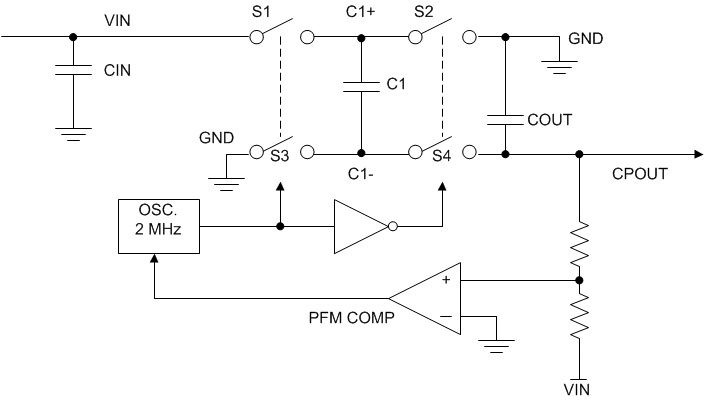
The voltage inverter portion of the LM27761 contains four large CMOS switches which are switched in sequence to invert the input supply voltage. Energy transfer and storage are provided by external capacitors. Figure 17 shows the voltage switches S2 and S4 are open. In the second time interval, S1 and S3 are open; at the same time, S2 and S4 are closed, and C1 is charging C3. After a number of cycles, the voltage across C3 is pumped into VIN. Because the anode of C3 is connected to ground, the output at the cathode of C3 equals –(VIN) when there is no load current. When a load is added the output voltage drop is determined by the parasitic resistance (RDSON of the MOSFET switches and the equivalent series resistance (ESR) of the capacitors) and the charge transfer loss between the capacitors.
 Figure 17. Voltage Inverting Principle
The output characteristic of this circuit can be approximated by an ideal voltage source in series with a resistance. The voltage source equals –(VIN). The output resistance ROUT is a function of the ON resistance of the internal MOSFET switches, the oscillator frequency, the capacitance, and the ESR of C1 and C3. Because the switching current charging and discharging C1 is approximately twice as the output current, the effect of the ESR of the pumping capacitor C1 is multiplied by four in the output resistance. The charge-pump output capacitor C3 is charging and discharging at a current approximately equal to the output current; therefore, its ESR only counts once in the output resistance. A good approximation of charge-pump ROUT is shown in Equation 1:
where
- RSW is the sum of the ON resistance of the internal MOSFET switches shown in Figure 17.
High capacitance and low-ESR ceramic capacitors reduce the output resistance.