SNVSA85C October   2015  – January 2017 LM27761

PRODUCTION DATA.  

  1. Features
  2. Applications
  3. Description
    1.     Device Images
      1.      Typical Application
  4. Revision History
  5. Pin Configuration and Functions
    1.     Pin Functions
  6. Specifications
    1. 6.1 Absolute Maximum Ratings
    2. 6.2 ESD Ratings
    3. 6.3 Recommended Operating Conditions
    4. 6.4 Thermal Information
    5. 6.5 Electrical Characteristics
    6. 6.6 Typical Characteristics
  7. Detailed Description
    1. 7.1 Overview
    2. 7.2 Functional Block Diagram
    3. 7.3 Feature Description
      1. 7.3.1 Undervoltage Lockout
      2. 7.3.2 Input Current Limit
      3. 7.3.3 PFM Operation
      4. 7.3.4 Output Discharge
      5. 7.3.5 Thermal Shutdown
    4. 7.4 Device Functional Modes
      1. 7.4.1 Shutdown Mode
      2. 7.4.2 Enable Mode
  8. Application and Implementation
    1. 8.1 Application Information
    2. 8.2 Typical Application - Regulated Voltage Inverter
      1. 8.2.1 Design Requirements
      2. 8.2.2 Detailed Design Procedure
        1. 8.2.2.1 Custom Design With WEBENCH® Tools
        2. 8.2.2.2 Charge-Pump Voltage Inverter
        3. 8.2.2.3 Negative Low-Dropout Linear Regulator
        4. 8.2.2.4 Power Dissipation
        5. 8.2.2.5 Output Voltage Setting
        6. 8.2.2.6 External Capacitor Selection
          1. 8.2.2.6.1 Charge-Pump Output Capacitor
          2. 8.2.2.6.2 Input Capacitor
          3. 8.2.2.6.3 Flying Capacitor
          4. 8.2.2.6.4 LDO Output Capacitor
      3. 8.2.3 Application Curves
  9. Power Supply Recommendations
  10. 10Layout
    1. 10.1 Layout Guidelines
    2. 10.2 Layout Example
  11. 11Device and Documentation Support
    1. 11.1 Device Support
      1. 11.1.1 Development Support
        1. 11.1.1.1 Custom Design With WEBENCH® Tools
    2. 11.2 Receiving Notification of Documentation Updates
    3. 11.3 Community Resources
    4. 11.4 Trademarks
    5. 11.5 Electrostatic Discharge Caution
    6. 11.6 Glossary
  12. 12Mechanical, Packaging, and Orderable Information

パッケージ・オプション

メカニカル・データ(パッケージ|ピン)
サーマルパッド・メカニカル・データ
発注情報

Pin Configuration and Functions

DSG Package
8-Pin WSON With Thermal Pad
Top View
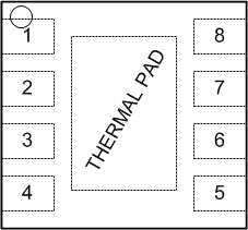
LM27761 packdraw.gif

Pin Functions

PINTYPE(1)DESCRIPTION
NUMBERNAME
1 VIN P Positive power supply input.
2 GND G Ground
3 CPOUT P Negative unregulated output voltage.
4 VOUT P Regulated negative output voltage.
5 VFB P Feedback input. Connect VFB to an external resistor divider between VOUT and GND. DO NOT leave unconnected.
6 EN I Active high enable input.
7 C1– P Negative terminal for C1.
8 C1+ P Positive terminal for C1.
Thermal Pad G Ground. DO NOT leave unconnected.
P: Power; G: Ground; I: Input.