SNOSC48O June 2000 – December 2014 LM2936
PRODUCTION DATA.
6 Specifications
6.1 Absolute Maximum Ratings (1)(2)
| MIN | MAX | UNIT | |
|---|---|---|---|
| Input voltage (survival) | −50 | 60 | V |
| Power dissipation (3) | Internally limited | ||
| Junction temperature (TJMAX) | 150 | °C | |
| Storage temperature, Tstg | −65 | 150 | |
(1) Absolute Maximum Ratings indicate limits beyond which damage to the device may occur. DC and AC electrical specifications do not apply when operating the device beyond its specified operating ratings.
(2) If Military/Aerospace specified devices are required, please contact the TI Sales Office/ Distributors for availability and specifications.
(3) The maximum power dissipation is a function of TJ(MAX), RθJA, and TA. The maximum allowable power dissipation at any ambient temperature is PD = (TJ(MAX) − TA) / RθJA. If this dissipation is exceeded, the die temperature can rise above the TJ(MAX) of 150°C, and the LM2936 may go into thermal shutdown.
6.2 ESD Ratings
| VALUE | UNIT | |||
|---|---|---|---|---|
| V(ESD) | Electrostatic discharge | Human-body model (HBM), per ANSI/ESDA/JEDEC JS-001(1) | ±2000 | V |
(1) JEDEC document JEP155 states that 500-V HBM allows safe manufacturing with a standard ESD control process. .
6.3 Recommended Operating Conditions
| MIN | MAX | UNIT | |
|---|---|---|---|
| Temperature, TJ | −40 | 125 | °C |
| Input voltage, VIN , LM2936 | 5.5 | 40 | V |
| Input voltage, VIN , LM2936HV only | 5.5 | 60 | V |
| Shutdown pin voltage, VSD, LM2936BM only | 0 | 40 | V |
6.4 Thermal Information
| THERMAL METRIC(1) | LM2936 | UNIT | |||||
|---|---|---|---|---|---|---|---|
| SOIC (D) | TO-252 (NDP) | VSSOP (DGK) | SOT-223 (DCY) | TO-92 (LP) | |||
| 8 PINS | 3 PINS | 8 PINS | 4 PINS | 3 PINS | |||
| RθJA | Junction-to-ambient thermal resistance | 111.4 | 50.5 | 173.4 | 62.8 | 156.8 | °C/W |
| RθJC(top) | Junction-to-case (top) thermal resistance | 56.3 | 52.6 | 65.9 | 44.2 | 80.4 | |
| RθJB | Junction-to-board thermal resistance | 51.9 | 29.7 | 94.9 | 11.7 | n/a | |
| ψJT | Junction-to-top characterization parameter | 10.9 | 4.8 | 9.6 | 3.6 | 24.5 | |
| ψJB | Junction-to-board characterization parameter | 51.4 | 29.3 | 93.3 | 11.6 | 136.0 | |
| RθJC(bot) | Junction-to-case (bottom) thermal resistance | n/a | 1.6 | n/a | n/a | n/a | |
(1) For more information about traditional and new thermal metrics, see the IC Package Thermal Metrics application report, SPRA953.
6.5 Electrical Characteristics for 3-V LM2936
VIN = 14 V, IOUT = 10 mA, TJ = 25°C, unless otherwise specified.| PARAMETER | TEST CONDITIONS | MIN(1) | TYP(2) | MAX(1) | UNIT |
|---|---|---|---|---|---|
| 3-V LM2936HV ONLY | |||||
| Output voltage | 5.5 V ≤ VIN ≤ 48 V, 100 µA ≤ IOUT ≤ 50 mA,(2) –40°C ≤ TJ ≤ 125°C | 2.91 | 3 | 3.09 | V |
| Line regulation | 6 V ≤ VIN ≤ 60 V, IOUT = 1 mA | 10 | 30 | mV | |
| ALL 3-V LM2936 | |||||
| Output voltage | 2.94 | 3 | 3.06 | V | |
| 4 V ≤ VIN ≤ 26 V, 100 µA ≤ IOUT ≤ 50 mA,(2) –40°C ≤ TJ ≤ 125°C | 2.91 | 3.000 | 3.09 | ||
| Quiescent current | IOUT = 100 μA, 8 V ≤ VIN ≤ 24 V | 15 | 20 | μA | |
| IOUT = 10 mA, 8 V ≤ VIN ≤ 24 V | 0.2 | 0.5 | mA | ||
| IOUT = 50 mA, 8 V ≤ VIN ≤ 24 V | 1.5 | 2.5 | mA | ||
| Line regulation | 9 V ≤ VIN ≤ 16 V | 5 | 10 | mV | |
| 6 V ≤ VIN ≤ 40 V, IOUT = 1 mA | 10 | 30 | |||
| Load regulation | 100 μA ≤ IOUT ≤ 5 mA | 10 | 30 | mV | |
| 5 mA ≤ IOUT ≤ 50 mA | 10 | 30 | |||
| Dropout voltage | IOUT = 100 μA | 0.05 | 0.1 | V | |
| IOUT = 50 mA | 0.20 | 0.40 | V | ||
| Short-circuit current | VOUT = 0 V | 65 | 120 | 250 | mA |
| Output impedance | IOUT = 30 mAdc and 10 mArms, ƒ = 1000 Hz | 450 | mΩ | ||
| Output noise voltage | 10 Hz–100 kHz | 500 | μV | ||
| Long-term stability | 20 | mV/1000 Hr | |||
| Ripple rejection | Vripple = 1 Vrms, ƒripple = 120 Hz | −40 | −60 | dB | |
| Reverse polarity transient input voltage |
RL = 500 Ω, t = 1 ms | −50 | −80 | V | |
| Output voltage with reverse polarity input |
VIN = −15 V, RL = 500 Ω | 0 | −0.3 | V | |
| Maximum Line Transient | RL = 500 Ω, VOUT ≤ 3.3 V, T = 40 ms | 60 | V | ||
| Output bypass capacitance (COUT) ESR |
COUT = 22 µF, 0.1 mA ≤ IOUT ≤ 50 mA | 0.3 | 8 | Ω | |
| SHUTDOWN INPUT − 3-V LM2936BM ONLY | |||||
| Output voltage, VOUT | Output off, VSD = 2.4 V, RLOAD = 500 Ω | 0 | 0.01 | V | |
| Shutdown high threshold voltage, VIH |
Output off, RLOAD = 500 Ω | 2 | 1.1 | V | |
| Shutdown low threshold voltage, VIL |
Output on, RLOAD = 500 Ω | 1.1 | 0.6 | V | |
| Shutdown high current, IIH |
Output off, VSD = 2.4 V, RLOAD = 500Ω | 12 | μA | ||
| Quiescent current | Output off, VSD = 2.4 V, RLOAD = 500 Ω, includes IIH current | 30 | μA | ||
(1) Datasheet min/max specification limits are ensured by design, test, or statistical analysis.
(2) Typicals are at 25°C (unless otherwise specified) and represent the most likely parametric norm.
6.6 Electrical Characteristics for 3.3-V LM2936
VIN = 14 V, IOUT = 10 mA, TJ = 25°C, unless otherwise specified.| PARAMETER | TEST CONDITIONS | MIN(1) | TYP(2) | MAX(1) | UNIT |
|---|---|---|---|---|---|
| 3.3-V LM2936HV ONLY | |||||
| Output voltage | 5.5 V ≤ VIN ≤ 48 V, 100 µA ≤ IOUT ≤ 50 mA,(3) –40°C ≤ TJ ≤ 125°C | 3.201 | 3.300 | 3.399 | V |
| Line regulation | 6 V ≤ VIN ≤ 60 V, IOUT = 1 mA | 10 | 30 | mV | |
| ALL 3.3-V LM2936 | |||||
| Output voltage | 3.234 | 3.300 | 3.366 | V | |
| 4 V ≤ VIN ≤ 26 V, 100 µA ≤ IOUT ≤ 50 mA,(3) –40°C ≤ TJ ≤ 125°C | 3.201 | 3.300 | 3.399 | ||
| Quiescent current | IOUT = 100 μA, 8 V ≤ VIN ≤ 24 V | 15 | 20 | μA | |
| IOUT = 10 mA, 8 V ≤ VIN ≤ 24 V | 0.2 | 0.5 | mA | ||
| IOUT = 50 mA, 8 V ≤ VIN ≤ 24 V | 1.5 | 2.5 | mA | ||
| Line regulation | 9 V ≤ VIN ≤ 16 V | 5 | 10 | mV | |
| 6 V ≤ VIN ≤ 40 V, IOUT = 1 mA | 10 | 30 | |||
| Load regulation | 100 μA ≤ IOUT ≤ 5 mA | 10 | 30 | mV | |
| 5 mA ≤ IOUT ≤ 50 mA | 10 | 30 | |||
| Dropout voltage | IOUT = 100 μA | 0.05 | 0.10 | V | |
| IOUT = 50 mA | 0.2 | 0.4 | V | ||
| Short-circuit current | VOUT = 0 V | 65 | 120 | 250 | mA |
| Output impedance | IOUT = 30 mAdc and 10 mArms, ƒ = 1000 Hz | 450 | mΩ | ||
| Output noise voltage | 10 Hz–100 kHz | 500 | μV | ||
| Long-term stability | 20 | mV/1000 Hr | |||
| Ripple rejection | Vripple = 1 Vrms, ƒripple = 120 Hz | −40 | −60 | dB | |
| Reverse polarity transient input voltage |
RL = 500 Ω, T = 1 ms | −50 | −80 | V | |
| Output voltage with reverse polarity input |
VIN = −15 V, RL = 500 Ω | 0 | −0.3 | V | |
| maximum line transient | RL = 500 Ω, VOUT ≤ 3.63 V, T = 40 ms | 60 | V | ||
| Output bypass capacitance (COUT) ESR |
COUT = 22 µF, 0.1 mA ≤ IOUT ≤ 50 mA | 0.3 | 8 | Ω | |
| SHUTDOWN INPUT − 3.3-V LM2936BM ONLY | |||||
| Output voltage, VOUT | Output off, VSD = 2.4 V, RLOAD = 500 Ω | 0 | 0.01 | V | |
| Shutdown high threshold voltage, VIH |
Output off, RLOAD = 500 Ω | 2 | 1.1 | V | |
| Shutdown low threshold voltage, VIL |
Output on, RLOAD = 500 Ω | 1.1 | 0.6 | V | |
| Shutdown high current, IIH |
Output off, VSD = 2.4V, RLOAD = 500 Ω | 12 | μA | ||
| Quiescent current | Output off, VSD = 2.4V, RLOAD = 500 Ω, includes IIH current | 30 | μA | ||
(1) Datasheet min/max specification limits are ensured by design, test, or statistical analysis.
(2) Typicals are at 25°C (unless otherwise specified) and represent the most likely parametric norm.
(3) To ensure constant junction temperature, pulse testing is used.
6.7 Electrical Characteristics for 5-V LM2936
VIN = 14 V, IOUT = 10 mA, TJ = 25°C, unless otherwise specified.| PARAMETER | TEST CONDITIONS | MIN(1) | TYP(2) | MAX(1) | UNIT |
|---|---|---|---|---|---|
| 5-V LM2936HV ONLY | |||||
| Output voltage | 5.5 V ≤ VIN ≤ 48 V, 100 µA ≤ IOUT ≤ 50 mA,(3) –40°C ≤ TJ ≤ 125°C | 4.85 | 5 | 5.15 | V |
| Line regulation | 6 V ≤ VIN ≤ 60 V, IOUT = 1 mA | 15 | 35 | mV | |
| ALL 5-V LM2936 | |||||
| Output voltage | 4.9 | 5 | 5.1 | V | |
| 5.5 V ≤ VIN ≤ 26 V, 100 µA ≤ IOUT ≤ 50 mA,(3) –40°C ≤ TJ ≤ 125°C | 4.85 | 5 | 5.15 | ||
| Quiescent current | IOUT = 100 μA, 8 V ≤ VIN ≤ 24 V | 9 | 15 | μA | |
| IOUT = 10 mA, 8 V ≤ VIN ≤ 24 V | 0.2 | 0.5 | mA | ||
| IOUT = 50 mA, 8 V ≤ VIN ≤ 24 V | 1.5 | 2.5 | mA | ||
| Line regulation | 9 V ≤ VIN ≤ 16 V | 5 | 10 | mV | |
| 6 V ≤ VIN ≤ 40 V, IOUT = 1 mA | 10 | 30 | |||
| Load regulation | 100 μA ≤ IOUT ≤ 5 mA | 10 | 30 | mV | |
| 5 mA ≤ IOUT ≤ 50 mA | 10 | 30 | |||
| Dropout voltage | IOUT = 100 μA | 0.05 | 0.1 | V | |
| IOUT = 50 mA | 0.2 | 0.4 | V | ||
| Short-circuit current | VOUT = 0 V | 65 | 120 | 250 | mA |
| Output impedance | IOUT = 30 mAdc and 10 mArms, ƒ = 1000 Hz | 450 | mΩ | ||
| Output noise voltage | 10 Hz–100 kHz | 500 | μV | ||
| Long-term stability | 20 | mV/1000 Hr | |||
| Ripple rejection | Vripple = 1 Vrms, ƒripple = 120 Hz | −40 | −60 | dB | |
| Reverse polarity transient input voltage |
RL = 500 Ω, T = 1 ms | −50 | −80 | V | |
| Output voltage with reverse polarity input |
VIN = −15 V, RL = 500 Ω | 0 | −0.3 | V | |
| Maximum line transient | RL = 500 Ω, VOUT ≤ 5.5 V, T = 40 ms | 60 | V | ||
| Output bypass capacitance (COUT) ESR |
COUT = 10 µF, 0.1 mA ≤ IOUT ≤ 50 mA | 0.3 | 8 | Ω | |
| SHUTDOWN INPUT − 5-V LM2936BM ONLY | |||||
| Output voltage, VOUT | Output off, VSD = 2.4 V, RLOAD = 500 Ω | 0 | 0.01 | V | |
| Shutdown high threshold voltage, VIH |
Output off, RLOAD = 500 Ω | 2 | 1.1 | V | |
| Shutdown low threshold voltage, VIL |
Output on, RLOAD = 500 Ω | 1.1 | 0.6 | V | |
| Shutdown high current, IIH |
Output off, VSD = 2.4 V, RLOAD = 500 Ω | 12 | μA | ||
| Quiescent current | Output off, VSD = 2.4 V, RLOAD = 500Ω, includes IIH current | 30 | μA | ||
(1) Datasheet min/max specification limits are ensured by design, test, or statistical analysis.
(2) Typicals are at 25°C (unless otherwise specified) and represent the most likely parametric norm.
(3) To ensure constant junction temperature, pulse testing is used.
6.8 Typical Characteristics
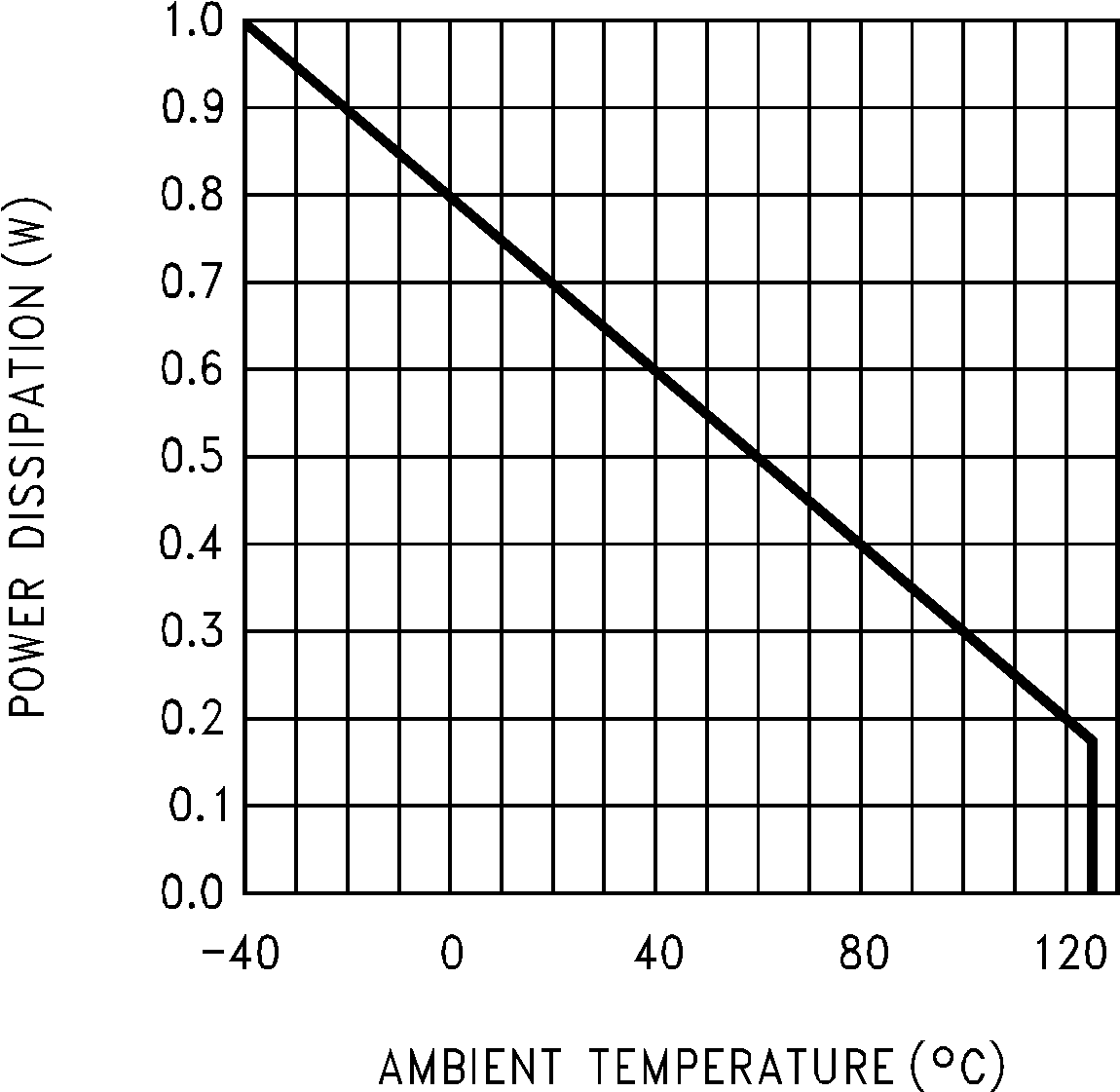 Figure 1. Maximum Power Dissipation (TO-92)
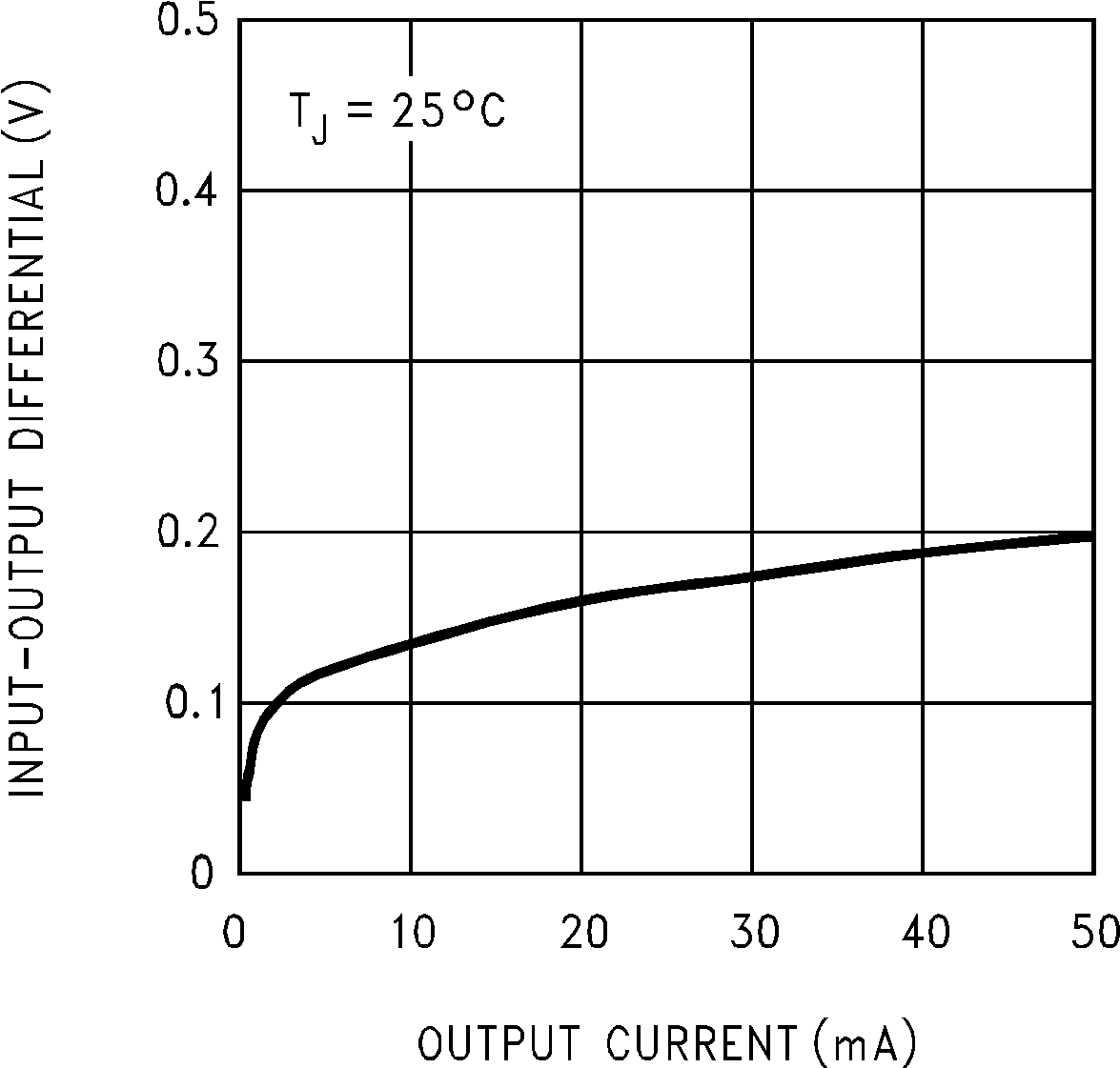 Figure 3. Dropout Voltage
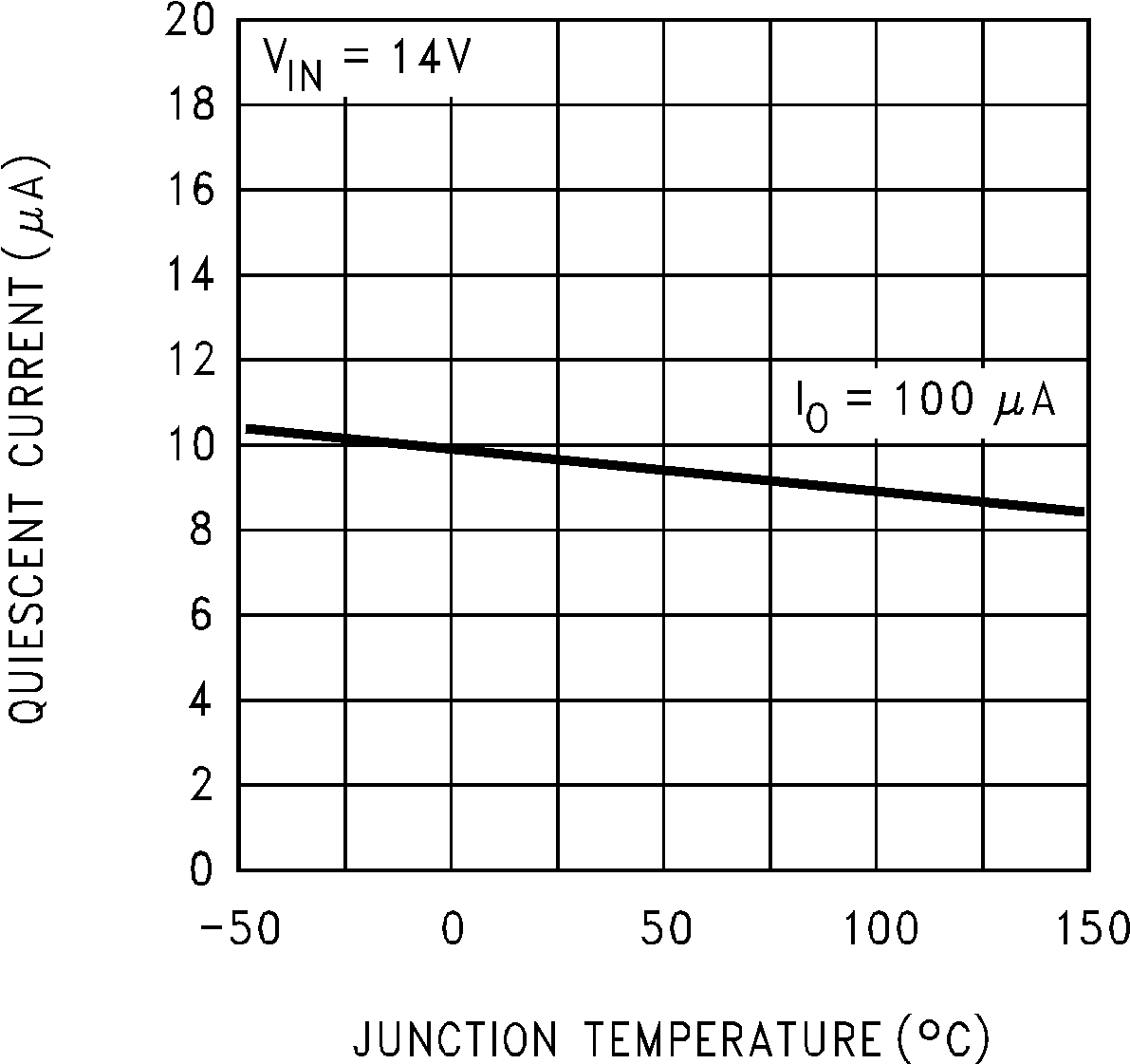 Figure 5. Quiescent Current
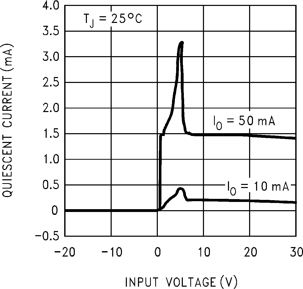 Figure 7. Quiescent Current
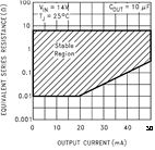 Figure 9. 5-V LM2936 COUT ESR
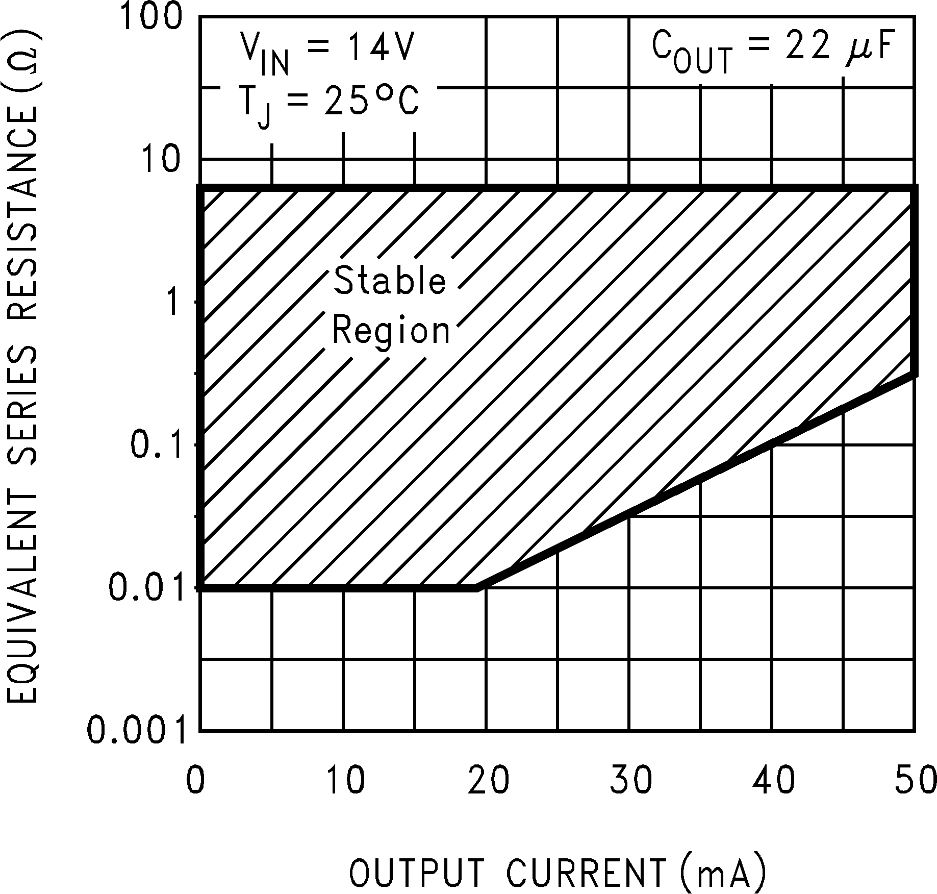 Figure 11. 3.3-V LM2936 COUT ESR
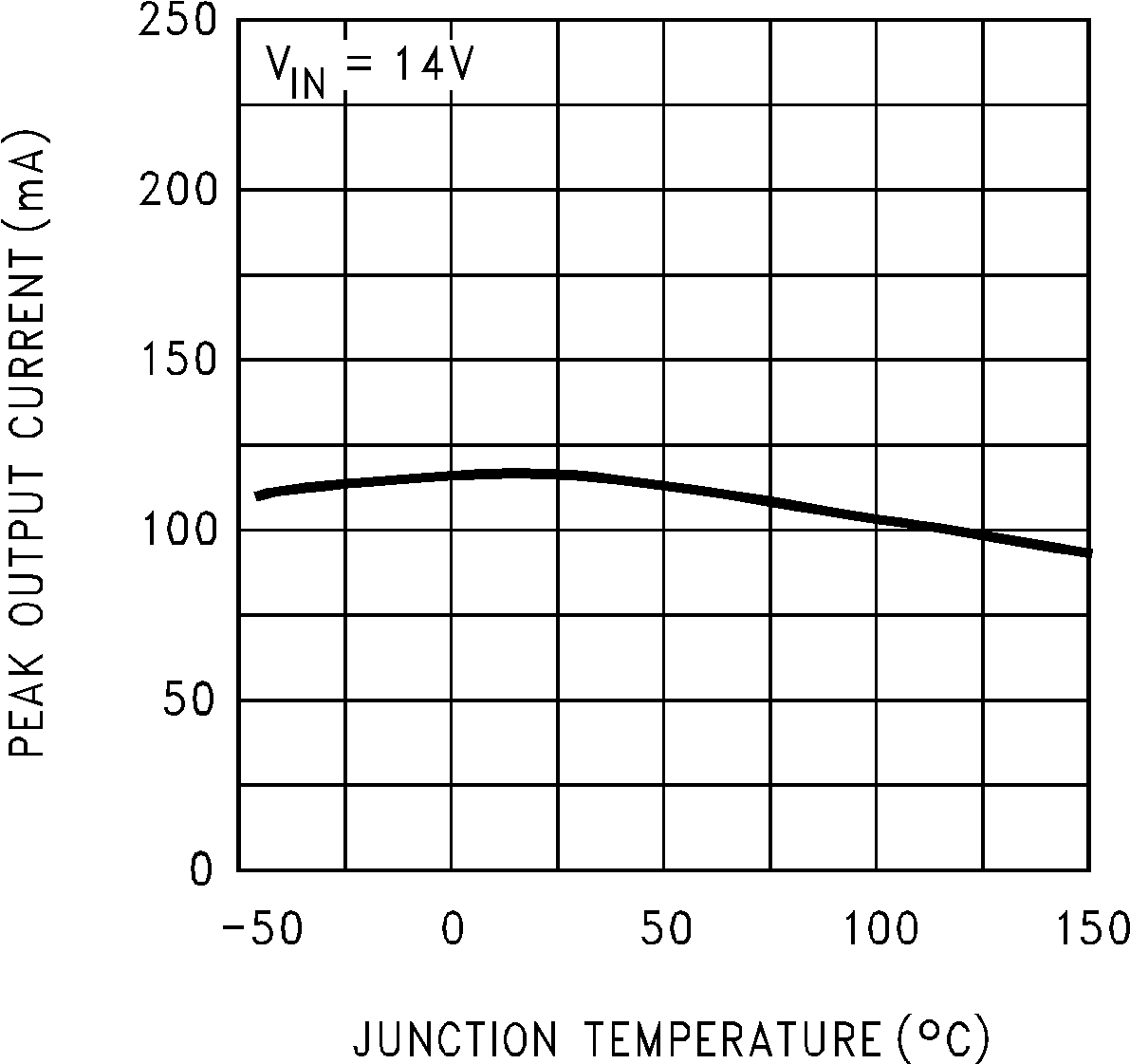 Figure 13. Peak Output Current
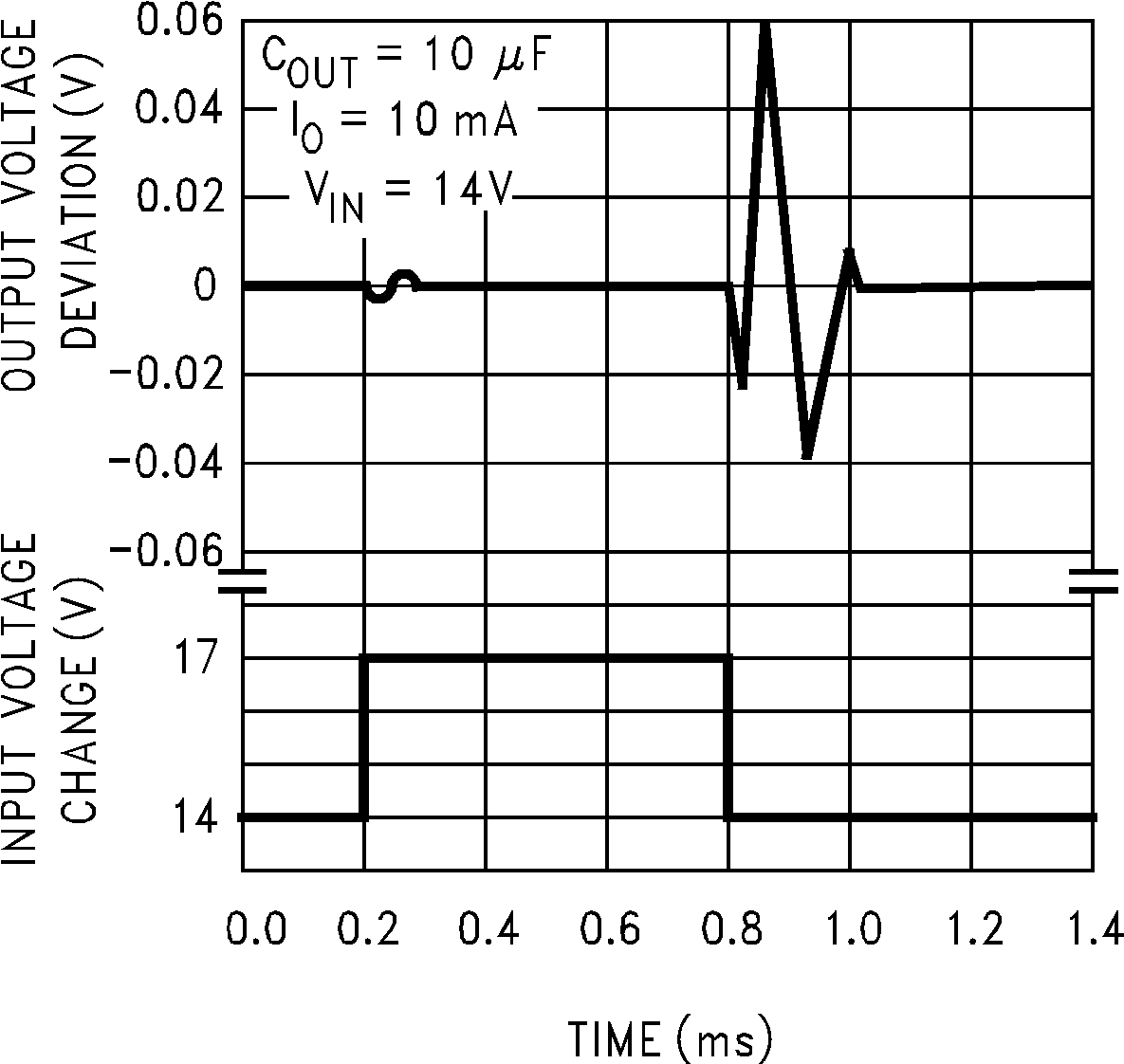 Figure 15. 5-V LM2936 Line Transient Response
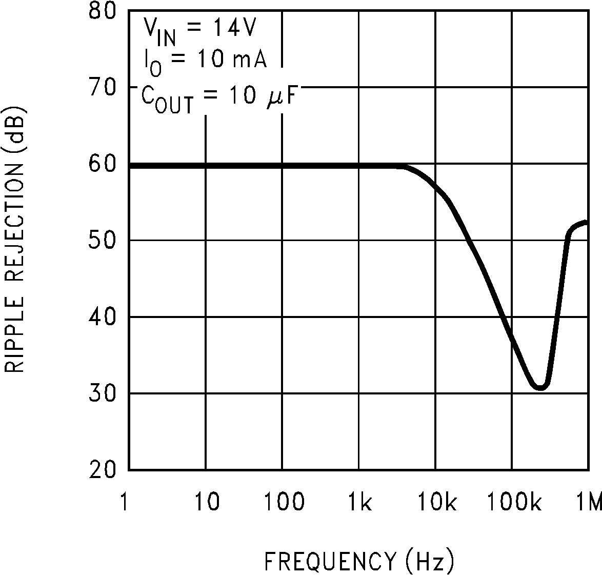 Figure 17. 5-V LM2936 Ripple Rejection
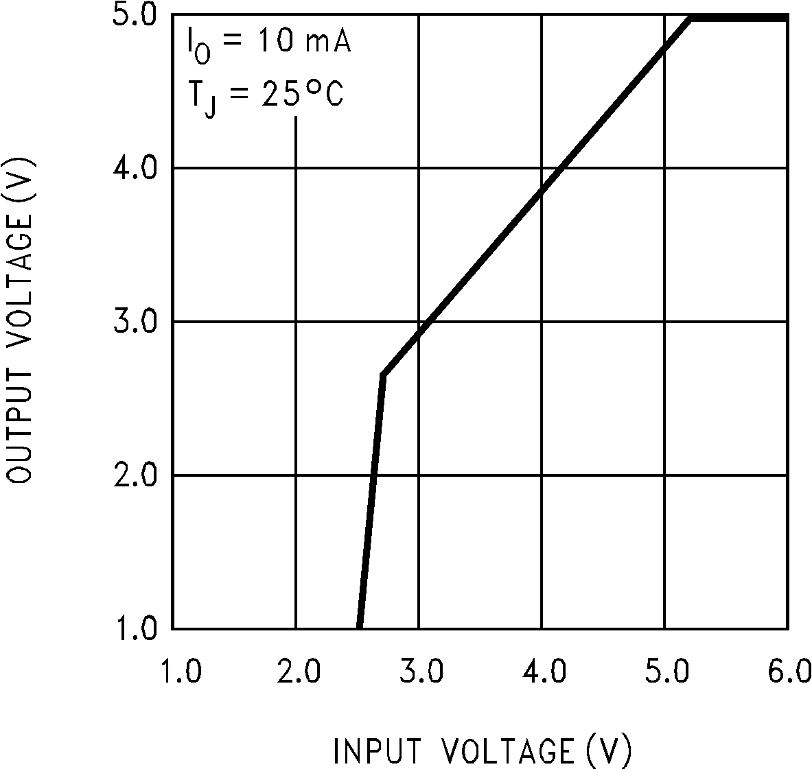 Figure 19. 5-V LM2936 Low Voltage Behavior
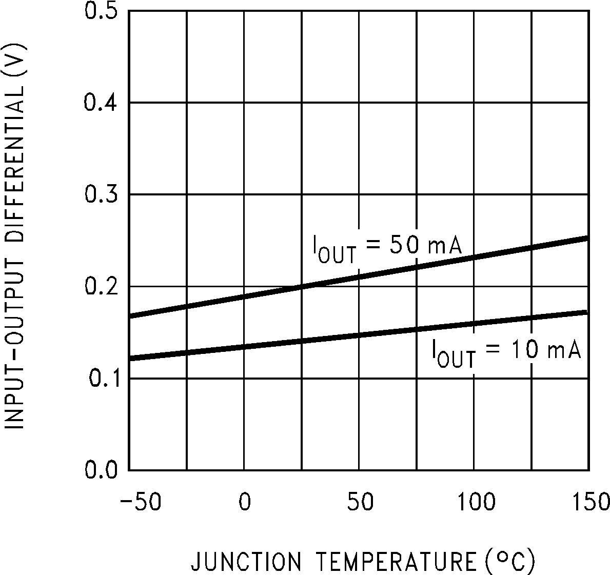 Figure 2. Dropout Voltage
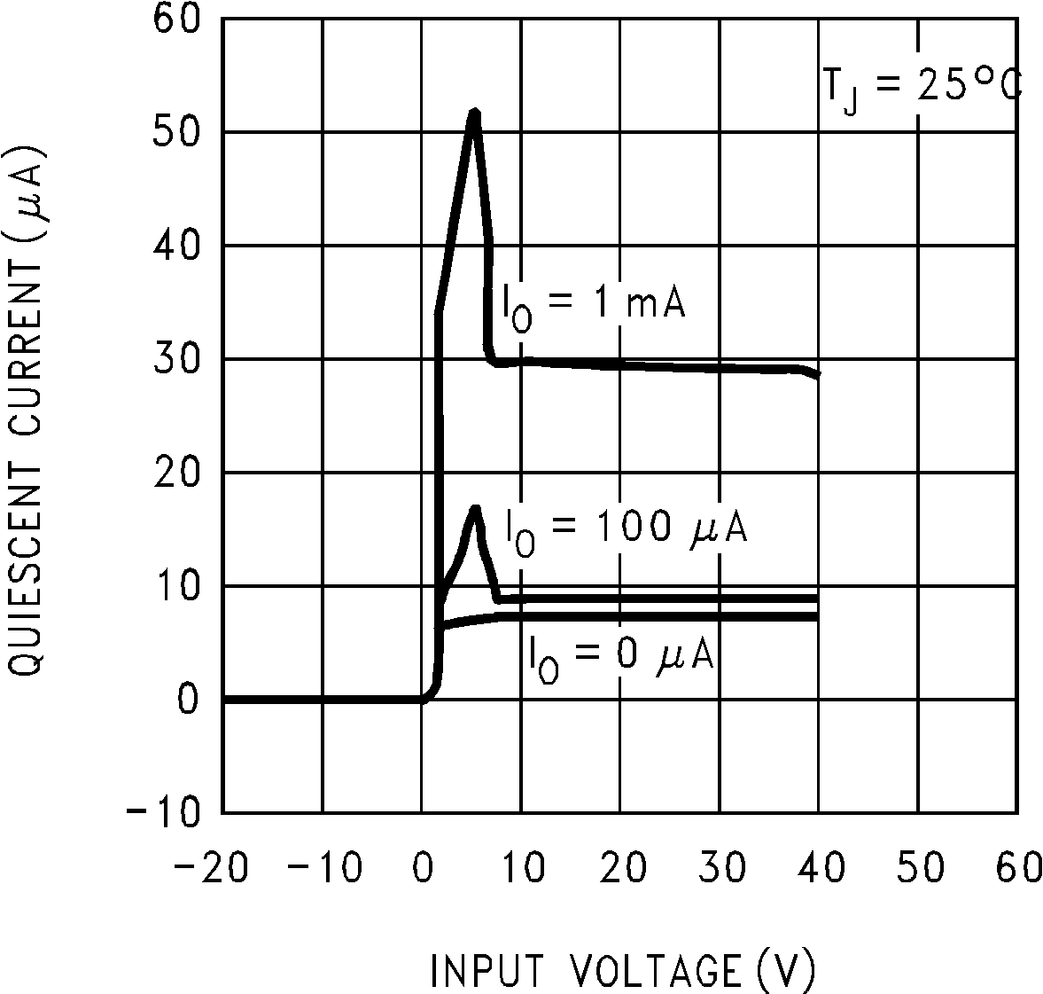 Figure 4. Quiescent Current
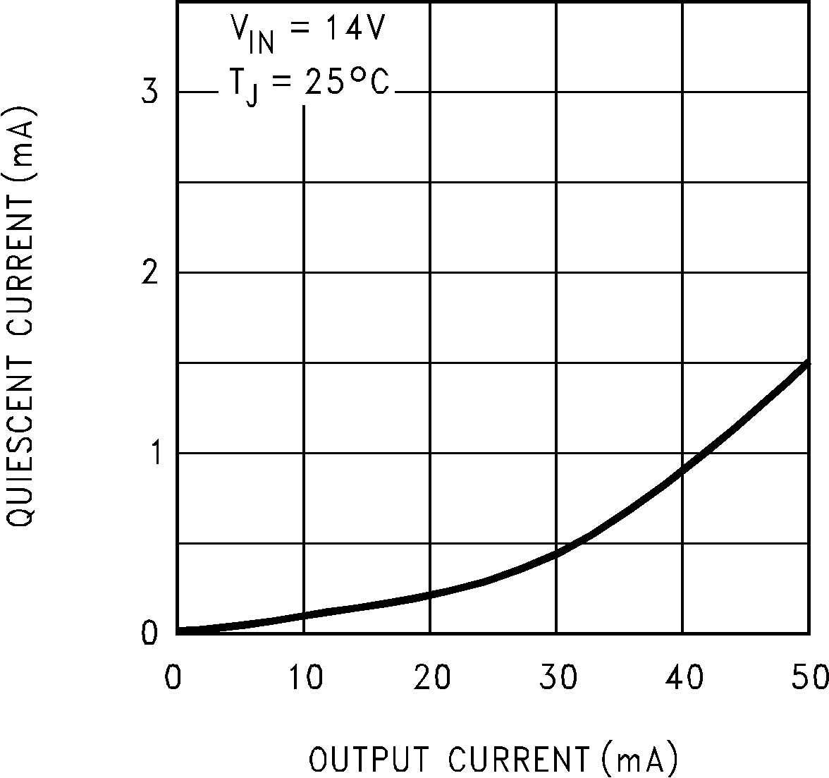 Figure 6. Quiescent Current
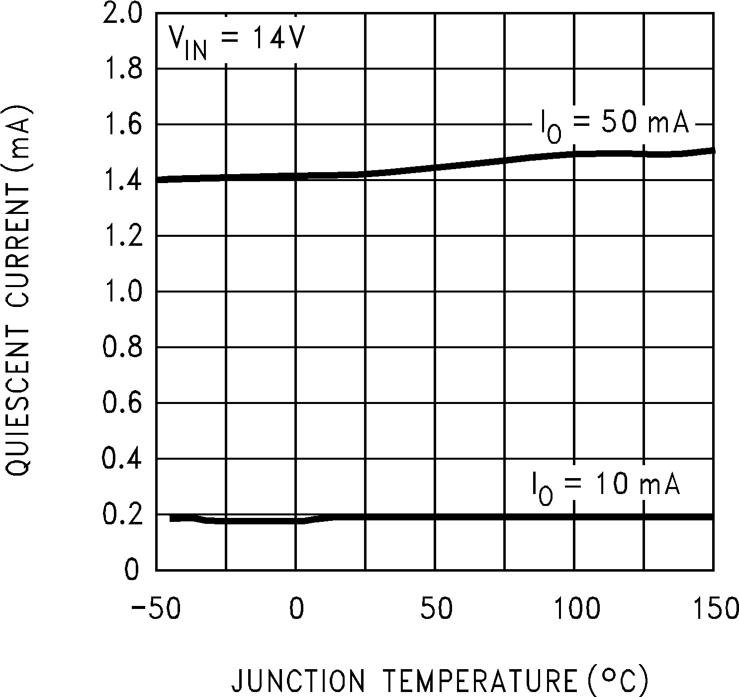 Figure 8. Quiescent Current
 Figure 10. 3-V LM2936 COUT ESR
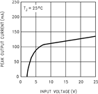 Figure 12. Peak Output Current
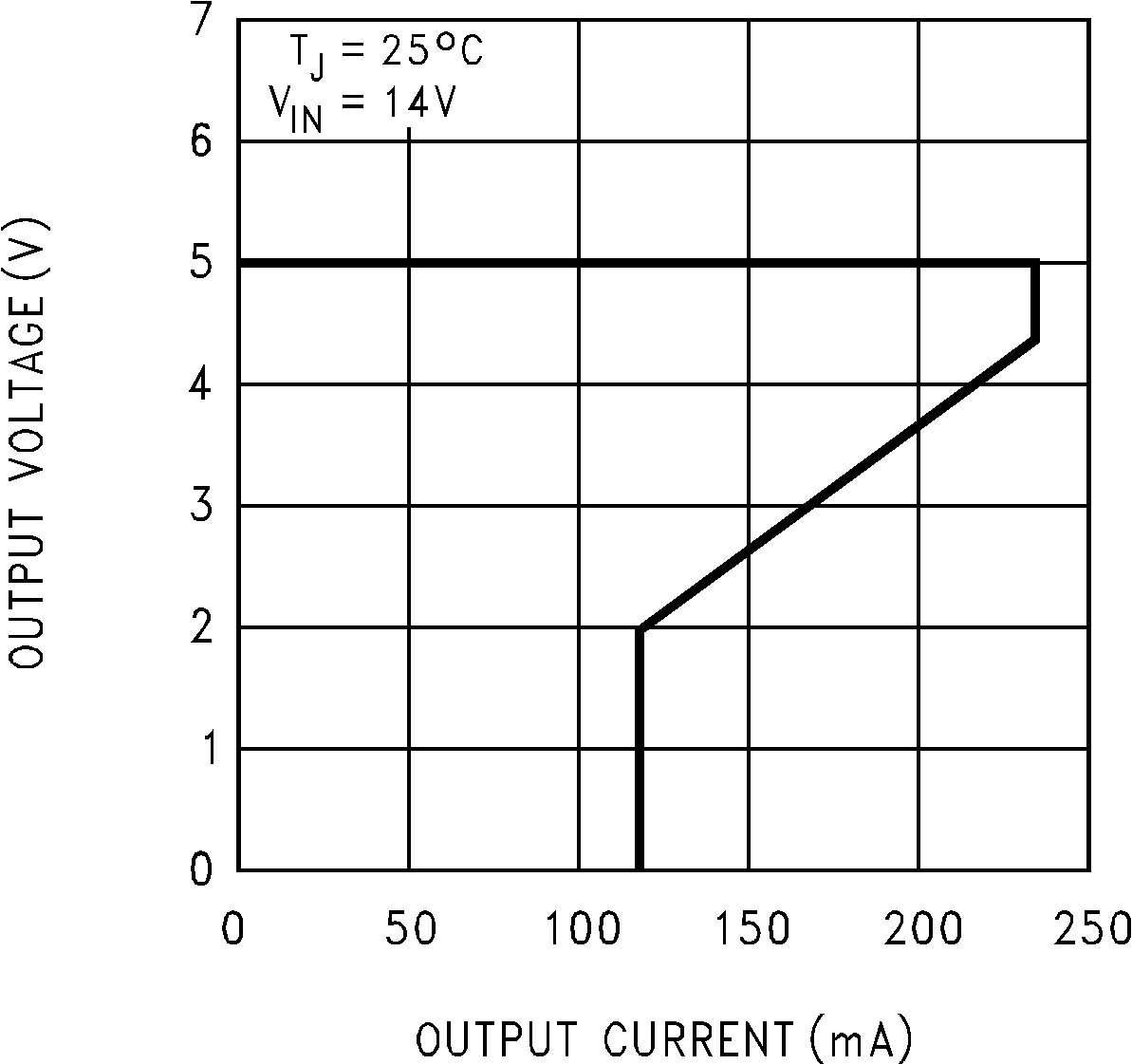 Figure 14. 5-V LM2936 Current Limit
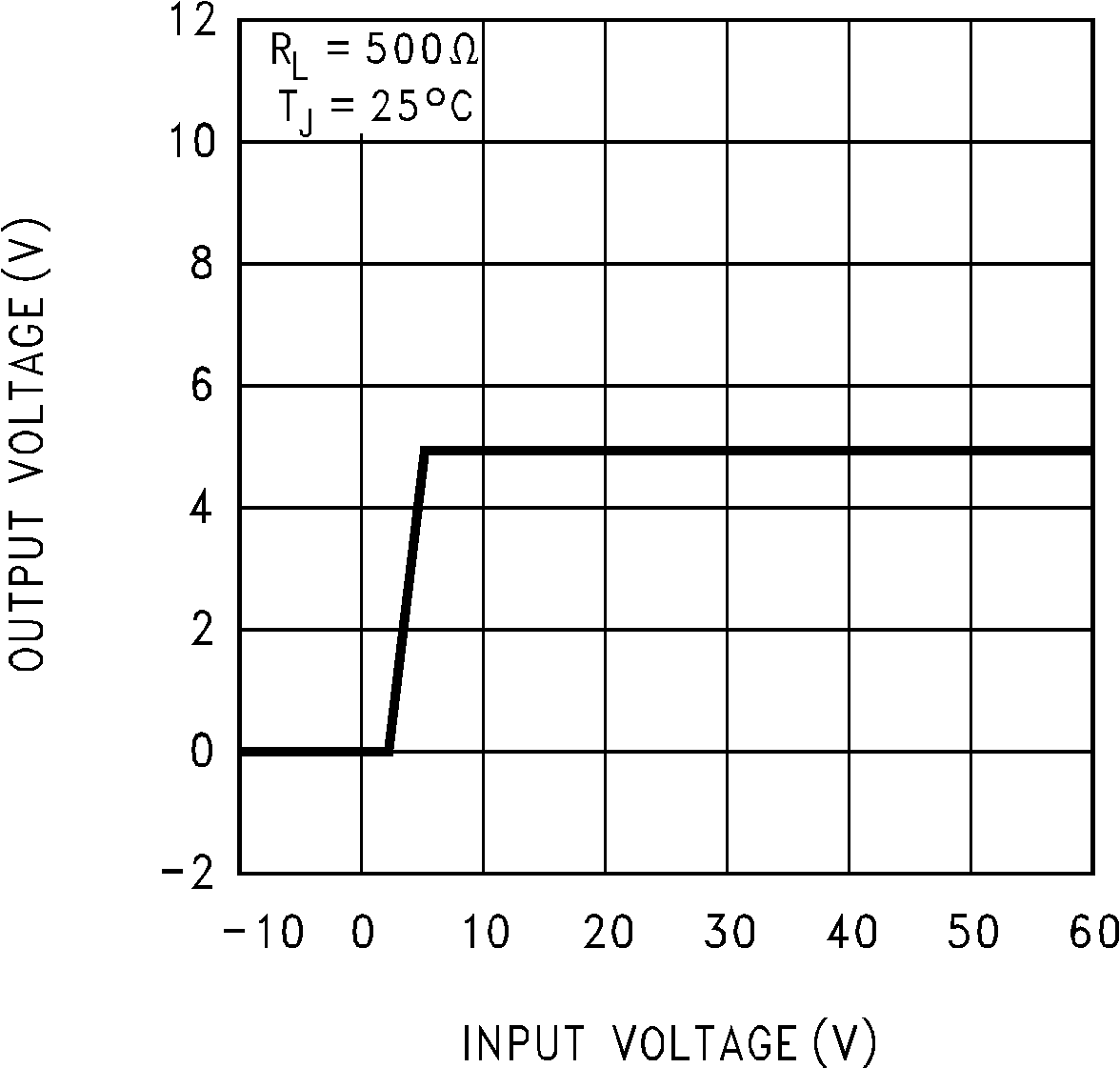 Figure 16. 5-V LM2936 Output at Voltage Extremes
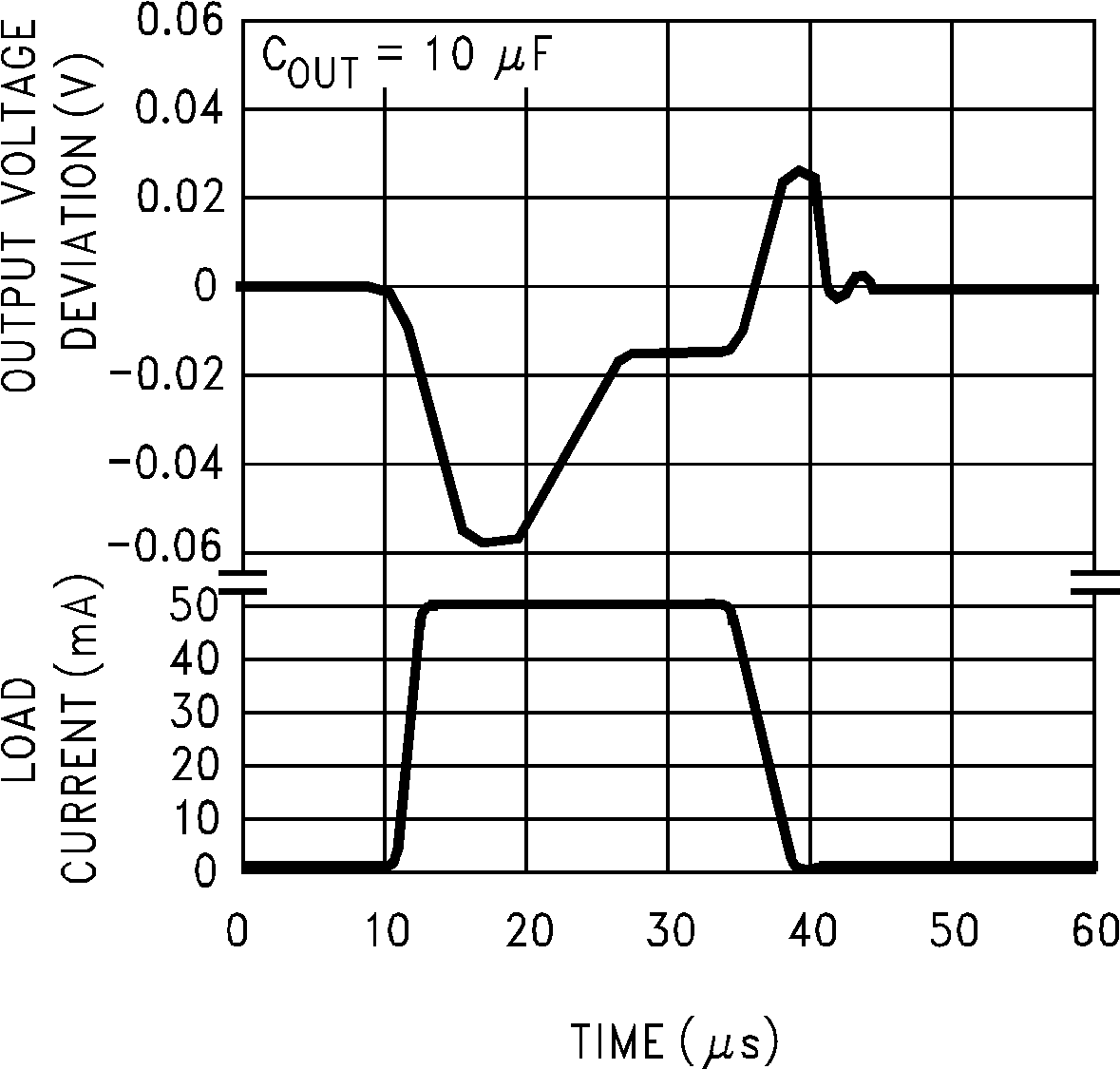 Figure 18. 5-V LM2936 Load Transient Response
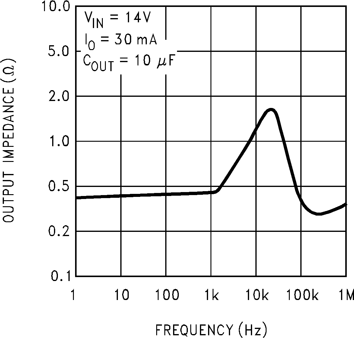 Figure 20. 5-V LM2936 Output Impedance