SNVS684D November 2010 – March 2016
PRODUCTION DATA.
- 1 Features
- 2 Applications
- 3 Description
- 4 Revision History
- 5 Pin Configuration and Functions
- 6 Specifications
- 7 Detailed Description
- 8 Application and Implementation
- 9 Power Supply Recommendations
- 10Layout
- 11Device and Documentation Support
- 12Mechanical, Packaging, and Orderable Information
パッケージ・オプション
メカニカル・データ(パッケージ|ピン)
サーマルパッド・メカニカル・データ
発注情報
8 Application and Implementation
NOTE
Information in the following applications sections is not part of the TI component specification, and TI does not warrant its accuracy or completeness. TI’s customers are responsible for determining suitability of components for their purposes. Customers should validate and test their design implementation to confirm system functionality.
8.1 Application Information
The LM2936Q ultralow quiescent current regulator features low dropout voltage and low current in the standby mode. The LM2936Q has a 40-V maximum operating voltage limit, a −40°C to +125°C operating temperature range, –24-V input transient protection, and ±3% output voltage tolerance over the entire output current, input voltage, and temperature range The WEBENCH® software may be used to generate complete designs. When generating a design, WEBENCH utilizes iterative design procedure and accesses comprehensive databases of components. See www.ti.com for more details.
8.2 Typical Application
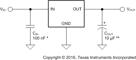
Figure 20 shows the typical application circuit for the LM2936Q. For the LM2936Q 5-V option, the output capacitor, COUT, must have a capacitance value of at least 10 µF with an equivalent series resistance (ESR) of at least 0.3 Ω, but no more than 8 Ω. For the LM2936Q 3-V and 3.3-V options, the output capacitor, COUT, must have a capacitance value of at least 22 µF with an ESR of at least 0.3 Ω, but no more than 8 Ω. The minimum capacitance value and the ESR requirements apply across the entire expected operating ambient temperature range.

8.2.1 Design Requirements
Table 1. Design Parameters
| DESIGN PARAMETER | EXAMPLE VALUE |
|---|---|
| Input voltage | 5.5 V to 40 V |
| Output voltage | 5 V |
| Output current requirement | 1 mA to 50 mA |
| Input capacitor | 0.1 µF |
| Output capacitance | 10 µF minimum |
| Output capacitor ESR value | 0.3 Ω to 8 Ω |
8.2.2 Detailed Design Procedure
8.2.2.1 External Capacitors
The output capacitor is critical to maintaining regulator stability, and must meet the required conditions for both ESR and minimum amount of capacitance.
8.2.2.1.1 Minimum Capacitance
The minimum output capacitance required to maintain stability is at least 10 µF for the LM2936Q 5-V option, and at least 22 µF for the 3-V and 3.3-V options. This value may be increased without limit. Larger values of output capacitance will give improved transient response.
8.2.2.1.2 ESR Limits
The ESR of the output capacitor causes loop instability if it is too high, or too low. The ESR of the COUT capacitor must at least 0.3 Ω, but no more than 8 Ω.
8.2.2.2 Output Capacitor ESR
It is essential that the output capacitor meet the capacitance and ESR requirements, or oscillations can result. The ESR is used with the output capacitance in order to produce a zero in the control loop frequency response. This zero increases phase margin and ensures stability of the output voltage. Refer to ESR, Stability, and the LDO Regulator (SLVA115) for details.
Ceramic capacitors (MLCC) can be used for COUT only if a series resistor is added to simulate the ESR requirement. The ESR is not optional — it is mandatory. Typically, a 500-mΩ to 1-Ω series resistor is used for this purpose. When using MLCCs, due diligence must be given to initial tolerances, capacitance derating due to applied DC voltage, and capacitance variations due to temperature. Dielectric types X5R and X7R are preferred.
8.2.2.3 Power Dissipation
Knowing the device power dissipation and proper sizing of the thermal plane connected to the tab or pad is critical to ensuring reliable operation. Device power dissipation depends on input voltage, output voltage, and load conditions and can be calculated with Equation 1.
Power dissipation can be minimized, and greater efficiency can be achieved, by using the lowest available voltage drop option that would still be greater than the dropout voltage (VDO). However, keep in mind that higher voltage drops result in better dynamic (that is, PSRR and transient) performance.
On the 8-pin SOIC (D) package, the four ground pins are thermally connected to the backside of the die. Adding approximately 0.04 square inches of 2 oz. copper pad area to these four pins improves the JEDEC RθJA rating from 111.4°C/W to approximately 100°C/W. If this extra copper area is placed directly beneath the SOIC package there should not be any impact on board density.
Power dissipation and junction temperature are most often related by the junction-to-ambient thermal resistance (RθJA) of the combined PCB and device package and the temperature of the ambient air (TA), according to Equation 2 or Equation 2:
Unfortunately, this RθJA is highly dependent on the heat-spreading capability of the particular PCB design, and therefore varies according to the total copper area, copper weight, and location of the planes. The RθJA recorded in Thermal Information is determined by the specific EIA/JEDEC JESD51-7 standard for PCB and copper-spreading area, and is to be used only as a relative measure of package thermal performance. For a well-designed thermal layout, RθJA is actually the sum of the package junction-to-case (bottom) thermal resistance (RθJCbot) plus the thermal resistance contribution by the PCB copper area acting as a heat sink.
8.2.2.4 Estimating Junction Temperature
The EIA/JEDEC standard recommends the use of psi (Ψ) thermal characteristics to estimate the junction temperatures of surface mount devices on a typical PCB board application. These characteristics are not true thermal resistance values, but rather package specific thermal characteristics that offer practical and relative means of estimating junction temperatures. These psi metrics are determined to be significantly independent of copper-spreading area. The key thermal characteristics (ΨJT and ΨJB) are given in Thermal Information and are used in accordance with Equation 4 or Equation 5.
where
- PD(MAX) is explained in Equation 3
- TTOP is the temperature measured at the center-top of the device package.
where
- PD(MAX) is explained in Equation 3.
- TBOARD is the PCB surface temperature measured 1-mm from the device package and centered on the package edge.
For more information about the thermal characteristics ΨJT and ΨJB, see Semiconductor and IC Package Thermal Metrics (SPRA953); for more information about measuring TTOP and TBOARD, see Using New Thermal Metrics (SBVA025); and for more information about the EIA/JEDEC JESD51 PCB used for validating RθJA, see Thermal Characteristics of Linear and Logic Packages Using JEDEC PCB Designs (SZZA017). These application notes are available at www.ti.com.
8.2.3 Application Curve
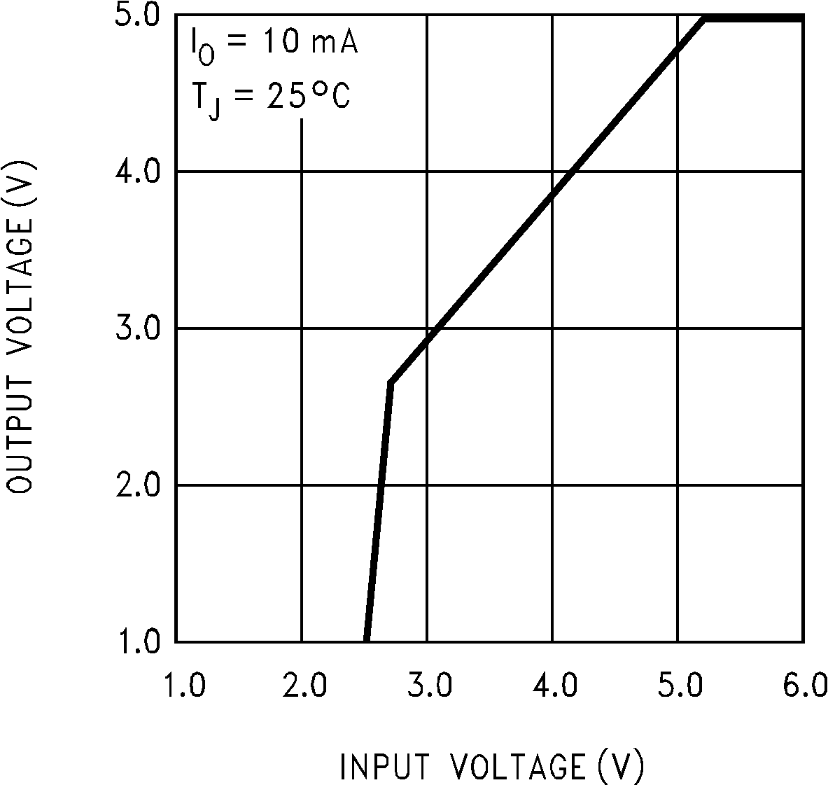
 Figure 21. LM2936Q VOUT vs VIN