SNVS684D November 2010 – March 2016
PRODUCTION DATA.
- 1 Features
- 2 Applications
- 3 Description
- 4 Revision History
- 5 Pin Configuration and Functions
- 6 Specifications
- 7 Detailed Description
- 8 Application and Implementation
- 9 Power Supply Recommendations
- 10Layout
- 11Device and Documentation Support
- 12Mechanical, Packaging, and Orderable Information
パッケージ・オプション
メカニカル・データ(パッケージ|ピン)
サーマルパッド・メカニカル・データ
発注情報
10 Layout
10.1 Layout Guidelines
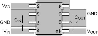
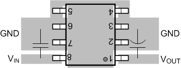
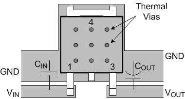
The dynamic performance of the LM2936Q is dependent on the layout of the PCB. PCB layout practices that are adequate for typical LDOs may degrade the PSRR, noise, or transient performance of the LM2936Q. Best performance is achieved by placing CIN and COUT on the same side of the PCB as the LM2936Q, and as close to the packageas is practical. The ground connections for CIN and COUT must be back to the LM2936Q ground pin using as wide and as short of a copper trace as possible.
Connections using long trace lengths, narrow trace widths, and/or connections through vias must be avoided as these add parasitic inductances and resistances that give inferior performance, especially during transient conditions.
10.2 Layout Examples
 Figure 22. LM2936QHBM SOIC (D) Layout
 Figure 23. LM2936QM SOIC (D) Layout
 Figure 24. LM2936Q TO-252 (NDP) Layout